Deactivation of Ultra Shallow B and BF2 Profiles After Non-Melt Laser Annealing
- PDF / 228,736 Bytes
- 5 Pages / 612 x 792 pts (letter) Page_size
- 63 Downloads / 239 Views
0912-C04-07
Deactivation of Ultra Shallow B and BF2 Profiles After Non-Melt Laser Annealing James A. Sharp1, Nicholas E.B Cowern1, Roger P. Webb1, Damiano Giubertoni2, Salvotore Gennaro2, Massimo Bersani2, Majeed A. Foad3, and Karen J. Kirkby1 1 Ion Beam Centre, Advanced Technology Institute, School of Electronics and Physical Sciences, University of Surrey, Guildford, Surrey, GU2 7XH, United Kingdom 2 ITC-irst, Trento, 38050, Italy 3 Applied Implant Technologies, 974 E. Arques Avenue, Sunnyvale, California, 94086
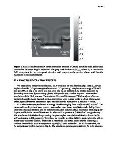
ABSTRACT Ultra-shallow B and BF2 implants in silicon pre-amorphised with Ge have been activated using a scanning non-melt laser. The implants were activated either by using 1 or 10 laser scans. Isochronal 60s post-laser annealing between 700-1000ºC were then undertaken to study the deactivation and reactivation of the B. Both B and BF2 samples were implanted with a dose of 1x10¹⁵ B cm-2 at an effective energy of 500eV. The presence of F from the BF2 implants, which is superimposed over the boron profile increases the sheet resistance of the initial fabricated junction (from 600-700 ohms/sq from B implants only to 750-1100 ohms/sq for BF2 implants). Fluorine also changes the deactivation and reactivation behaviour of the boron during the postanneals by increasing the amount of deactivation of the boron.
INTRODUCTION The continued aggressive scaling down of source and drain extension regions for CMOS devices requires ultra shallow and abrupt profiles that have a low sheet resistance [1]. Boron implanted at very low energies (sub 1 keV) in conjunction with pre-amorphising implants can obtain the required junction depths for the PMOS source/drain extension regions, provided that diffusion is minimal and activation of the dopant is high. However, problems arise as a consequence of excess silicon interstitials in the tail region of the pre-amorphizing implant, which agglomerate into end-of-range (EOR) defects just beyond the depth of the initial amorphous/crystalline interface. These defects ripen and dissolve during annealing, releasing interstitials which diffuse back towards the surface, and react with the implanted B atoms. These reactions lead to transient enhanced diffusion (TED) [2] and the creation of boron interstitial clusters (BICs) which reduce the active doping level in the peak region of the B profile [3,4]. As the anneal temperature or time is increased, reactivation occurs where the BICs dissolve, releasing interstitials [3,4]. To minimize such problems, an ultra-short time/high temperature anneal can be used to anneal the pre-amorphized B implant. Since B-interstitial coupling is weaker at high temperatures, TED and deactivation are expected to be reduced for the same amount of EOR defect annealing. In this case, however, it is important to assess the deactivation that may occur during subsequent thermal processing steps. A promising ultra-short high-temperature annealing approach is the non-melt scanning laser approach [5-6]. In this paper the de-activation/re-activation behaviour of B, usin
Data Loading...