Amorphous Silicon Based TFT and MIS Nonvolatile Memories
- PDF / 158,679 Bytes
- 6 Pages / 612 x 792 pts (letter) Page_size
- 18 Downloads / 379 Views
0989-A10-03
Amorphous Silicon Based TFT and MIS Nonvolatile Memories Yue Kuo, and Helinda Nominanda Texas A&M University, 235 J. E. Brown Engineering Bldg., MS 3122, College Station, TX, 77843-3122
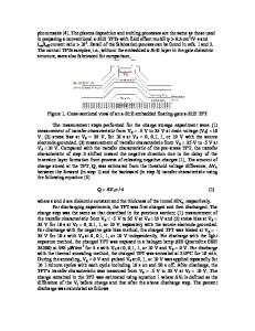
ABSTRACT The amorphous silicon (a-Si:H) TFT and MIS capacitor, which include an a-Si:H layer embedded in the silicon nitride gate dielectric layer, have been prepared and characterized for memory functions. Large shifts of the threshold voltage and flat band voltage were detected in the current-voltage and capacitance-voltage hysteresis measurements. The embedded a-Si:H film functioned as a charge retention medium that stores and releases injected carriers. The deviceís memory capacity varied with the thickness of the embedded a-Si:H layer and the sweep voltage. These low-cost memory devices can be used in many low-temperature prepared circuits. INTRODUCTION Due to its versatility in functions, e.g., as a pixel switching, reading or controlling device, the a-Si:H TFT has been used in both LCD and non-LCD products [1]. Recently, the non-volatile memory application of a-Si:H TFT has been demonstrated [2, 3]. The device utilizes a thin layer of hydrogenated amorphous silicon (a-Si:H) layer embedded inside the TFTís SiNx gate dielectric layer. The embedded a-Si:H layer serves as floating gate for charge trapping. The onepump down deposition of the gate dielectric, channel and passivation layers by PECVD method promotes clean interfaces as well as provided a simpler fabrication compared to other floating gate memory structure that utilizes separate patterning steps for the embedded layer [4]. The TFT memory can be used in LCD applications during the idle state that requires no data update. For non-LCD applications, TFT memory can act as an alternative built-in memory. Here, authors further investigated the charge trapping mechanism of the TFT-based memory device and examined the interface and bulk dielectric properties of the floating gate MIS capacitor memory device. For instance, influences of the embedded a-Si:H film thickness and the operating gate voltage (Vg) on interface density of states (Dit), flat-band voltages (VFB), flat-band voltage shifts (∆VFB), leakage current (Ioff), fixed charge density (Qot) were investigated. The relationship between the characteristics of the embedded a-Si:H MIS capacitor and TFT are discussed. EXPERIMENT The complete TFT for memory was fabricated following a self-aligned, inverted staggered, tri-layer TFT, two-photomask process on Corning 1737 glass [5]. Figure 1a shows the cross-section structure of the TFTñbased floating gate memory [2]. The gate, and later, the source and drain electrodes were made of 100-nm thick DC-sputtered molybdenum (Mo). The Mo layers were etched with a solution of CH3COOH:H3PO4:HNO3:H2O. The gate dielectric was composed of 150 nm SiNx/4, 7, or 9 nm thick intrinsic a-Si:H/150 nm SiNx layers. For comparison, the TFT with no embedded a-Si:H layer was also fabricated, as shown in Fig. 1b. A
50-nm thick undoped a-Si:H layer for channel and a 250-nm thick SiNx for
Data Loading...