Amorphous Silicon Crystallization for TFT Applications
- PDF / 1,019,772 Bytes
- 6 Pages / 414.72 x 648 pts Page_size
- 105 Downloads / 415 Views
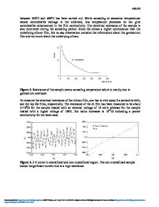
ABSTRACT Thin film hydrogenated amorphous silicon (a-Si:H) was deposited on molybdenum (Mo) substrates by d.c. glow discharge. We investigated the a-Si:H crystallization using four anneal techniques; nitrogen atmosphere furnace, vacuum, rapid thermal anneal (RTA), and excimer laser anneal. Anneal temperature ranged from 100 to 1200 'C. Excimer laser energy per pulse ranged from 90 to 340 mJ. Transmission electron microscopy (TEM) revealed microstructure of crystallized Si film with grain size over 0.5 pim. X-ray diffraction (XRD) and Raman spectroscopy were employed to determine the degree of crystallization. The a-Si:H started to crystallize at temperatures over 600 'C. An 850 'C anneal reduced film resistivity to 10' (0-cm) for intrinsic and 1 (fl-cm) for n-type. Coplanar type thin film transistors (TFT) with gate channel length of 25 pm and width of 220 pm were fabricated with various insulating layers; rf sputtered Si0 2, Si3N4, BaTiO 3, MgO, and evaporated SiO. The first two exhibited the least leakage current. 2 The as-grown intrinsic a-Si:H field effect mobility was around 0.03 (cm N.s) and delay time was 7 5x10" s. The solid phase crystallized silicon film exhibited high leakage current. The delay time 7 of an excimer laser anneal treated TFT was reduced to 2.5x10" s. Crystallized Si film mobility 2 N.s). (cm was improved to 15 INTRODUCTION
In the early 1970's, Spear and Lecomber showed that a-Si:H could be doped and demonstrated MOS transistor-like field effect devices [1]. Probably the most promising application of a-Si:H thin film transistors (TFTs) is their use in addressable liquid crystal displays. Intrinsic a-Si:H shows weak n-type conductivity, hence TFTs operate in the electron accumulation mode. TFTs for flat panel displays requires the following properties: high Ioo ratio of 10i; high off resistance 2 10" (01); and a low, stable threshold voltage (VT) - 5 (V) for Si0 2 dielectric; 2 high field effect mobility ) 1 (cm N.s). Achieving high ON current depends mainly on obtaining high field effect mobility by optimizing the a-Si:H layer, the gate dielectric layer, and the interface between them. Achieving high OFF resistance can be achieved using a very thin semiconductor layer to increase the OFF resistance. Finally, threshold voltage is a strong influenced function of the fixed charge in the gate and passivation of dielectric and is strongly 2 by the deposition process. The low field effect mobility in a-Si:H (0.3-1.5 cm N.s) has long been an obstacle to many practical applications. Recently, various technologies which improve the field effect mobility of poly-Si TFTs have been reported such as low pressure chemical vapor deposited (LPCVD) poly-Si, solid phase crystallization, laser crystallization, and hydrogenation [2-5]. This paper reports the mobility improvement using various crystallization techniques. Increased mobility can contribute to increase the ON current and the switching speed of TFT's. 701 Mat. Res. Soc. Symp. Proc. Vol. 321. ©1994 Materials Research Society
EXPERIMENTAL Due to t
Data Loading...