Solid phase crystallization of hot-wire CVD amorphous silicon films
- PDF / 606,490 Bytes
- 6 Pages / 612 x 792 pts (letter) Page_size
- 33 Downloads / 461 Views
A10.5.1
Solid phase crystallization of hot-wire CVD amorphous silicon films
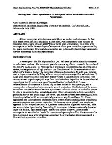
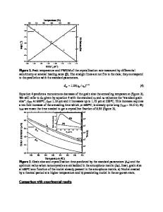
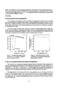
David L. Young, Paul Stradins, Eugene Iwaniczko, Bobby To, Bob Reedy, Yanfa Yan, Howard M. Branz, John Lohr2, Manuel Alvarez1, John Booske1 Amy Marconnet1 and Qi Wang National Renewable Energy Laboratory, 1617 Cole Blvd., Golden, CO 80401 1 Electrical and Computer Engineering, University of Wisconsin, 1415 Engineering Drive Madison, WI 53706 2 DIII-D National Fusion Facility, General Atomics, 3550 General Atomics Court, San Diego, California 92121-1122 ABSTRACT We measure times for complete solid phase crystallization (SPC) of hydrogenated amorphous silicon (a-Si:H) thin films that vary eight orders of magnitude, from a few ms to a few days. The time-to-crystallization activation energy is consistent with literature values of approximately 3.4 eV but the prefactor is markedly different for hot-wire chemical vapor deposition (HWCVD) films than for plasma-enhanced (PE) CVD films. The crystallized films were 0.3 – 2 µm thick, and deposited by high deposition rate (10-100 Å/s) HWCVD or standard PECVD onto glass substrates. We annealed these a-Si:H films over a wide temperature range (500 to 1100 ˚C) using techniques including simple hot-plates and tube furnaces, rapid thermal annealing by a tungsten-halogen lamp, and microwave electromagnetic heating at 2.45 GHz (magnetron) and 110 GHz (gyrotron). INTRODUCTION Interest in crystalline silicon thin-films on low-cost substrates for solar cells has driven research on solid phase crystallization (SPC) of amorphous silicon (a-Si) thin films on glass [1]. Polycrystalline thin films of silicon have better transport properties than hydrogenated amorphous silicon (a-Si:H) films [2], and are not subject to light-induced degradation effects. Low deposition (7 Å/s) rate, ~ 2µm thick a-Si:H films grown by PECVD and thermally crystallized have been shown to be of adequate electronic quality to produce 8-9% solar cell modules [1]. There is also considerable interest in developing inexpensive high-quality SPC films for large-area arrays of high-mobility thin-c-Si device transistors. Electronic-grade a-Si thin films are routinely deposited at rates between 1 – 10 Å/s by a variety of methods including plasma-enhanced chemical vapor deposition (PECVD). Hot-wire CVD (HWCVD) has been shown to produce good quality a-Si:H films at rates exceeding 130 Å/s, but with much higher microstructural disorder compared with films grown at lower rates or by other techniques [3]. In this paper we investigate SPC parameters of high (3%) microvoid density HWCVD a-Si:H thin films deposited at rates up to 100 Å/s. We annealed the films over a wide temperature range (500 to 1100 ˚C) and time range (ms to days) using a variety of techniques. An activation energy for the time-to-crystallization was measured over this large temperature range. Film quality after SPC shows promise for further study. In addition, we have performed preliminary experiments using high-power microwave sources to induce SPC of aSi:H.
A10.5.2
EXPERIMENT The a