Applications of Energy Beams in Material and Device Processing
- PDF / 1,879,587 Bytes
- 11 Pages / 417.6 x 639 pts Page_size
- 31 Downloads / 378 Views
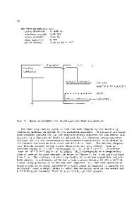
APPLICATIONS OF ENERGY BEAMS IN MATERIAL AND DEVICE PROCESSING G.J. GALVIN, L.S. HUNG, J.W. MAYER AND M. NASTASI Dept. of Materials Science and Engineering Cornell University, Ithaca, New York 14853 ABSTRACT Energetic ion beams used outside the traditional role of ion implantation are considered for semiconductor applications involving interface modification for self-aligned silicide contacts, composition modification for formation of buried oxide layers in Si on insulator structures and reduced disorder in high energy ion beam annealing for buried collectors in transistor fabrication. In metals, aside from their use in modification of the composition of near surface regions, energetic ion beams are being investigated for structural modification in crystalline to amorphous transitions. Pulsed beams of photons and electrons are used as directed energy sources in rapid solidification. Here, we consider the role of temperature gradients and impurities in epitaxial growth of silicon. INTRODUCTION Over the past five years, the modification of materials by energy beams - ions, photons, and electrons - has been the topic of MRS conferences [1-3], Ion Beam Modification of Materials Conferences [4,5], NATO Conferences on Materials Science [6] as well as the subject of edited volumes on surface modification [7] and laser annealing [8]. The 1983 MRS conference is no exception with six of the symposia either directed toward or containing sessions on beam modification and processing. This paper reviews some of the recent developments in materials and device processing. The traditional areas of ion implantation in semiconductors for controlled doping, laser processing of metal surfaces and ion beam metallurgy are well-established and the use of beam techniques is dependent on economic factors. Here we are concerned with developments that bear on future applications. The emphasis is on ion beams for interface and composition modification and on pulsed beams for the kinetics of epitaxial growth of semiconductors. INTERFACE MODIFICATION The penetration of energetic ion beams through the interface between deposited metal-films and the substrate leads to a modification of the interface. The improvement of adhesion by "ion stitching" has now received increased attention. In another area of application, ion irradiation has been used to aid the formation of uniform reacted layers as shown schematically in Fig. 1. The reaction of metal-films with semiconductors can proceed in an irregular, laterally-nonuniform fashion if there are contaminants or oxide patches at the interface between the metal-film and the semiconductor. The non-uniform reaction during annealing of deposited Al films in contact windows to Si etched in Si0 2 layers is commonly observed [9]. During thermal processing, Si diffuses from the exposed Si in the contact opening Mat. Res. Soc. Symp.
Proc. Vol. 23 (1984) (Elsevier
Science Publishing Co.,
Inc.
26
Metal
Thermal Anneal =
LSi,GaAs._ N-aotive Oxide
-Weak spots (or pinholes)
Re Regions
Ion beam ThermalMea An
Data Loading...