Automated Scanning Probe Microscopy for Combinatorial Polymer Research
- PDF / 296,475 Bytes
- 7 Pages / 612 x 792 pts (letter) Page_size
- 90 Downloads / 257 Views
0894-LL04-03.1
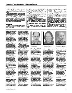
Automated Scanning Probe Microscopy for Combinatorial Polymer Research Daan Wouters,1 Alexander Alexeev,1,2 Dmitri Kozodaev,1,2 Sergey Saunin,2 Ulrich S. Schubert1,* 1 Laboratory of Macromolecular Chemistry and Nanoscience. Eindhoven University of Technology and the Dutch Polymer Institute (DPI), P.O. Box 513, 5600 MB, Eindhoven, The Netherlands. Fax: +31 40 247 4186; Tel: +31 40 247 5303; E-mail: [email protected] 2 NT-MDT Ltd. 103460 Moscow, Russia ABSTRACT With the development of combinatorial material research (CMR) methods and high throughput experimentation (HTE) workflows for polymer research applications, the increasing demand for automated, high throughput characterization methods is evident. Solution-based characterization methods like NMR, GPC, DSC, viscosimetry and UV-Vis as well as fluorescence plate readers are already available. Here we report on the incorporation of automated scanning probe microscopy in the HTE-workflow by demonstrating the evaluation of surface properties and topographies for thin polymer film libraries. INTRODUCTION Scanning probe microscopy (SPM) is a valuable tool in current polymer research. The technique is commonly used to evaluate surface properties of a large variety of polymer samples, revealing basic information, such as sample topography but also morphology, phase separation and local conductivity measurements. Traditionally, commercial SPM equipment is set up to work on small individual (~1 cm2) samples and operation requires a lot of user intervention. This and the fact that individual scans may take up to 10 minutes are the main reasons that SPM is not yet commonly used in high throughput experimentation workflows [1,2]. Other applications where automated SPM may be useful include scanning probe lithography work [3]. In this contribution, we introduce the application of an automated scanning probe microscope with custom modified software. Automated AFM is commonly developed for quality control purposes in the optical and the magnetic data storage industry operating on highly standardized sample formats [4]. Systems operating with parallel tips have also been reported but these require complicated operation and expensive microfabricated cantilevers [4, 5]. The presented system is capable of autonomous surface evaluation of large samples on different substrates in a sequential fashion, and its capabilities are demonstrated for three different experiments. EXPERIMENTAL DETAILS The machine used in the experiments consists of a modified SOLVER LS automated atomic force microscope from NT-MDT (Moscow, Russia), which is equipped with a scanner of 100 µm range and a large sample holder with programmable θY-stage of about 1 µm precision (see Figure 1).
0894-LL04-03.2
a) b) Figure 1. a) Modified SOLVER LS for automated measurements. b) Detail of the positioning platform for up to four 4-inch silicon wafers (right). By rotation and translation, each position on the stage is accessible for SPM-imaging. In the tailor-made software, a list of coordinates can be
Data Loading...