Rapid Thermal Annealing of Ion Implanted GaAs and InP
- PDF / 302,748 Bytes
- 6 Pages / 420.48 x 639 pts Page_size
- 6 Downloads / 373 Views
RAPID THERMAL ANNEALING OF ION IMPLANTED GaAs AND InP
K.V. Vaidyanathan and H.L. Dunlap Hughes Research Laboratories, 3011 Malibu Canyon Road Malibu, California 90265
ABSTRACT This paper discusses the properties of high intensity lamp-annealed silicon or beryllium-implanted GaAs and InP samples. We find this annealing process can result in efficient activation of dopants. Conventional furnace annealing at the same temperature does not result in increased electrical activation of the dopants. High fluence silicon implants can be activated in anneal times as short as 2 seconds, while low fluence silicon implants require more extended annealing. Activation of low fluence implants in GaAs depends strongly on the properties of the bulk semiinsulating material.
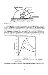
INTRODUCTION The process of ion implantation doping produces radiation damage in semiconductors. High temperature annealing is required in order to reduce this damage and to cause the dopants to occupy appropriate lattice sites to produce electrically active carriers in the material. In the case of compound semiconductors such as GaAs and InP, this carrier activation may be obtained only after annealing at temperatures where the material can undergo decomposition [1]. Careful control of the annealing atmosphere [2-4] and/or the use of an adequate encapsulant [5,6] has been required to prevent such material decomposition during the several minutes required for furnace anneals. One known exception to this has been the annealing behavior of beryllium-implanted GaAs and InP. This dopant can be activated at as low a 0 temperature as 500 C [7-9]. Transient beam processing techniques such as annealing with lasers or electron beams have shown mixed results. High carrier activation has been demonstrated but with extremely low carrier mobilities. The incident beam energy in these cases is absorbed in the near surface region of the semiconductor and results in differential heating of the semiconductor. This in turn introduces considerable stress into the implanted region', thus destroying the carrier mobility [10-12]. In this paper, we report on the application of a commercial system (HEATPULSETM, A.G. Associates) which uses high intensity lamps as a thermal source enabling the semiconductor to be brought rapidly to the desired anneal temperature within time periods of a few seconds. The period of heating during this process has been shown to be sufficiently long to result in heating the samples evenly but is short enough to alleviate the controlled atmosphere or encapsulant integrity requirements. We have used this annealing process to study the electrical activation behavior of Si (n-type) or Be (p-type) implanted semi-insulating GaAs and InP wafers. We find that this radiant annealing process can result in doped layers with electrical characteristics which are essentially indistinguishable from layers which have been conventionally furnace annealed at the same temperature.
Mat. Res.
Soc. Sytep. Proc. Vol.
23 (1984)@ Elsevier Science Publishing Co., Inc.
688
EXPER
Data Loading...