Characterization of Ni- and Ni(Pt)-Silicide Formation on Narrow Polycrystalline Si Lines by Raman Spectroscopy
- PDF / 448,333 Bytes
- 7 Pages / 420.48 x 639 pts Page_size
- 57 Downloads / 400 Views
tool for in-line process monitoring 4 . This nondestructive technique with micron spatial resolution can perform mapping analysis for phase identification on device structures, which provides useful information to the study of the reliability issue related to silicide and to correlate the microstructure with the sheet resistance5 . In this study, we present the results of micro-Raman study on the Ni and Ni(Pt) silicide formation on narrow polycrystalline Si (poly-Si) lines and pads. EXPERIMENT A layer of undoped poly-Si was deposited by LPCVD on a 400 nm thick oxide grown by furnace oxidation of the p-type (100) Si. The poly-Si was patterned into snake-like serpentine structures which consist of 120 runs with 70 J=m/run, giving a total length of 8400 rim. The polySi linewidth varies from 0.5 down to 0.25 Rm. 1Oxl00 Rm 2 poly-Si pads were also defined in the vicinity of the serpentine structures. After the poly-Si line patterning, tetraethylorthosilicate (TEOS) or nitride spacers were formed on the poly-Si sidewall. After a dilute HF dip, Ni and Ni(Pt) films of thickness 30 nm were blanket sputter deposited. Rapid thermal annealing (RTA) was carried out in N 2 ambient at temperatures ranging from 500 to 900'C for 60 s. The unreacted metal was then removed by selective etch using a H2SO 4 and H20 2 mixture. Micro-Raman measurements were done on the poly-Si serpentine structures and the polySi pads. Mapping analysis along n+ poly-Si lines was also performed to correlate with the sheet resistance measurements. The Raman spectra were recorded with a confocal spectrometer in backscattering configuration, fitted with single grating spectrographs, notch filters and charge coupled device (CCD) detector. A 513 nm Argon laser was used and focused to a spot diameter of about 1 jim. The sample is mounted on a computer controlled x-y motorized stage which allows mapping analysis to be performed on narrow lines at micron interval. An integration time of 300 s was used for these spectra with 1.0 cm 1 spectral resolution.
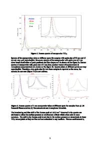
RESULTS Pure Ni silicide 2 Figure I(a) shows the Raman spectra from Ni salicided 100x 100 panm poly-Si pads after annealing at various temperatures. A strong peak at around 215 cm' is observed for the samples annealed at temperatures between 500 to 700°C. This peak has already been observed after annealing of Ni films on blanket (100)Si wafers and is characteristic of the presence of NiSi 6 . Thus, NiSi is present on the pads at temperatures ranging from 500 to 700°C. For poly-Si pads annealed at 750'C, the Raman spectrum shows 2 broad peaks between 250 to 450 cm 1 and a small peak at 230 cm 1 . These Raman peaks are identical to the ones observed for NiSi 2 on blanket (100)Si indicating the formation of NiSi 2 on the pads at 750'C. Figure 1(b) shows that the NiSi Raman peak intensity at 215 cm-l decreases continuously with increasing annealing temperature increases while the Si peak intensity at 520 cm-1 increases exponentially. This can be due to layer inversion 7 or agglomeration t . The decrease in the Si pea
Data Loading...