Dielectric Properties and Leakage Current Characteristics of Al 2 O 3 Thin Films with Thickness Variation
- PDF / 643,197 Bytes
- 6 Pages / 612 x 792 pts (letter) Page_size
- 34 Downloads / 408 Views
Dielectric Properties and Leakage Current Characteristics of Al2O3 Thin Films with Thickness Variation Jae-Hoon Choi, Ji-Woong Kim, and Tae-Sung Oh Department of Metallurgical Engineering and Materials Science, Hong Ik University, Seoul 121-791, Korea
ABSTRACT
Dielectric properties and leakage current characteristics of the Al2O3 thin films, deposited by reactive sputtering at room temperature, have been investigated with variations of the O2 content in the sputtering gas and the film thickness. The Al2O3 films of 10-300 nm thickness were amorphous without depending on the O2 contents of 25-75% in the sputtering gas. Maximum dielectric constant was obtained for the Al2O3 film deposited with the sputtering gas of 50% O2 content. With reduction of the film thickness from 300 nm to 10 nm, dielectric constant decreased from 9.04 to 3.71 and tangent loss increased from 0.0035 to 0.0594, respectively. When the O2 content in the sputtering gas was higher than 50%, the Al2O3 films exhibited no shift of the flatband voltage in C-V curves. The leakage current density increased with increasing the film thickness, and the Al2O3 films thinner than 100 nm exhibited the leakage current densities lower than 10-6 A/cm up to 650 kV/cm.
INTRODUCTION
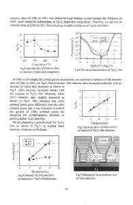
Al2O3 thin films have been investigated for many applications such as insulating materials, hard coatings, and diffusion barriers due to their attractive electrical and mechanical properties[1-3]. Al2O3 films have low permittivity to impurities such as alkali ions, high radiation resistance, relatively high dielectric constant, low dielectric loss, and relatively high thermal conductivity. Thus, application of Al2O3 films for dielectric materials in integrated circuits as gates and capacitors has attracted much attention in recent years[4]. Various deposition techniques such as sol-gel, metalorganic decomposition (MOD), sputtering, evaporation, metalorganic chemical vapor deposition (MOCVD), and pulsed laser ablation have been used to fabricate Al2O3 thin films[1-3]. Among these techniques, reactive sputtering has been widely used due to its high deposition rate and easy control of film composition. It has been also reported that the sputtered Al2O3 films exhibit superior chemical stability and mechanical strength compared to the films fabricated by other processes[2]. In this study, Al2O3 thin films of 10-30 nm thickness were deposited on Pt/Ti/SiO2/Si, Si, and Corning glass 2948 substrates by DC reactive sputtering at room temperature, and their electric characteristics were investigated with variations of the O2 content in the sputtering gas and the film thickness.
F3.5.1
EXPERIMENTAL PROCEDURE
Al target of 99.99% purity was used for reactive sputtering of Al2O3 thin films on the substrates of Pt(200 nm)/Ti(50 nm)/SiO2(300 nm)/Si(100), Si(100), and Corning glass 2948. After charging the substrates of 15 mm×15 mm size into the sputter chamber, Ar+ ion bombardment was conducted for 5 minutes with RF power of 100 W to remove the impurities and moisture absorbed on the substrate sur
Data Loading...