Characterization of Thin Dielectric Films as Copper Diffusion Barriers Using Triangular Voltage Sweep
- PDF / 3,005,482 Bytes
- 8 Pages / 417.6 x 639 pts Page_size
- 78 Downloads / 419 Views
ABSTRACT As technology progresses, the need for thinner Cu diffusion barrier caps is becoming more important, and it is advantageous if these barriers have low dielectric constants (K). Towards this end, we characterized Cu penetration in several thin (35 nm to 70 nm) dielectrics, including silicon nitrides, silicon oxynitrides, an amorphous hydrogenated carbon film, and a methyl silsesquioxane layer. Metal Insulator Silicon (MIS) structures were used as the test vehicle. The barrier dielectrics were deposited on 100 nm thermal oxide which was grown on 2 fl-cm, n-type Si wafers. After the deposition of 50 nm TEOS capping layers, both Al and Cu dots were evaporated on each wafer through a mask. Both Al and Cu dot samples were stressed at +2.7 MV/cm at 3000C for 10 minutes. For Cu dots, the applied stress pushed Cu ions into the dielectric stack. Stressing Al dots characterized the effects of the stress on the dielectric stacks and the quantity of Na ions in the films. Since C-V shifts are subject to stress-related instabilities in the interfaces as well as within the dielectrics themselves, triangular voltage sweep (TVS) was used after the applied stress to measure the concentration of Cu which reached the underlying thermal oxide film. The sensitivity of the TVS test with the structures used is about 5x1 09/cm 2 . Secondary ion mass spectroscopy (SIMS) analyses were performed on some of these samples to verify the electrical results.
INTRODUCTION As Cu back-end wiring and low-K integration merge in BEOL, more emphasis has to be placed on Cu encapsulation. In addition to corrosion and increased dielectric leakage, Cu has the potential to poison underlying active devices. Because of this, Cu barriers are important. Both dielectric and metal barriers are of use, so a quick, accurate technique for evaluating their effectiveness has to be demonstrated. Biasing Cu at an elevated temperature, so that it can move across these barriers, and then detecting the result of that movement is, in principle, how these barriers should be characterized. However, detecting the presence of Cu in dielectric layers beneath these barrier films is not always straightforward. Using extended stressing combined with leakage or time-dependent dielectric breakdown (TDDB) measurements' are time consuming and do not facilitate screening multiple dielectric barrier candidates. Observed flatband voltage shifts, determined with C-V measurements before and after bias temperature stress, is a technique which has been used to characterize Cu drift through dielectrics 2. It was observed that many dielectrics exhibit bulk, as well as interface, stress-related instabilities which can adversely influence the result of this test. Even if a film is
189
Mat. Res. Soc. Symp. Proc. Vol. 565 01999 Materials Research Society
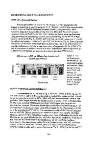
1.1
1.0 0.9 x 0.8 E 0.7
S0.6
-
Before Stress After Stress
0 0.5 0.4 0.3 0.2
-120 -100 -80 -60 -40 -20
0
Voltage (V)
Figure 1: C-V traces before and after bias temperature stress of +2 MV/cm at 300°C for 5 minutes for an Al dot/s
Data Loading...