Conducting Polypyrrole-based Field Effect Transistors Fabricated by Spin Coating and Inkjet Printing
- PDF / 98,817 Bytes
- 5 Pages / 612 x 792 pts (letter) Page_size
- 83 Downloads / 320 Views
I10.20.1
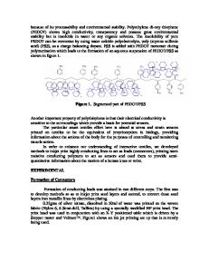
Conducting Polypyrrole-based Field Effect Transistors Fabricated by Spin Coating and Inkjet Printing Fengliang Xue, Yi Su, and Kody Varahramyan Institute for Micromanufacturing, Louisiana Tech University, Ruston, LA 71272, U.S.A ABSTRACT Spin coating and inkjet printing are two major deposition techniques for flexible polymer plastic electronics. This paper presents polymer field effect transistors (FET) fabricated by these two techniques using conducting poylmer polypyrole (PPy) as a semiconductor material. These thin film polymer field effect transistors operate in the depletion mode. The field effect mobilities are calculated to be 0.045 cm2 V-1s-1 and 0.036 cm2 V-1s-1, and transconductances are 0.104 µS and 0.096 µS at saturation region of the I-V curves for the spin coated and the inkjet printed transistors, respectively. The measured turn-off threshold voltage is around 20 V for both the spin coated and inkjet printed PPy FET transistors. The device performance of the spin coated transistors is slightly better than that of the inkjet printed transistors. This is mainly due to high surface roughness of the printed polymer film and printed dot boundaries, leading to low charge carrier mobility in the printed polymer FET transistors. INTRODUCTION Conducting and semiconducting conjugated polymers have been intensively investigated recently due to their possibility of replacing amorphous silicon thin film transistors for flat panel display application. The most promising soluble conducting polymers are poly(3,4ethylenedioxythiophene)–poly(styrenesulfonate) (PEDOT/PSS), polyaniline(PANI), and polypyrrole (PPy). These conducting polymers are suitable for spin coating and inkjet printing due to their low viscosity. PEDOT/PSS and PANI were reported to be semiconductor materials for field effect transistor application by means of line patterning and cast deposition techniques, respectively [1-2]. The field effect mobility of polyaniline was reported to be in a range of 10-3 to 10-6 cm2 V-1s-1depending on its doping level and heat treatment, while PEDOT/PSS polymer was reported to have an unbelievably high mobility of 170 cm2 V-1s-1 [2]. PPy polymer has been reported to be used as source/drain contact in field effect transistors [3], N2O gas sensing [4], and field effect devices [5-6]. The reported fabrication techniques for PPy polymer field effect transistors are based on line patterning technique [1] and electrochemical synthesis [6]. Chin-Tsuo Kou, et al [6] reported PPy field effect mobility in a range of 10-4 to 10 -3 cm2 V-1s-1 without heat treatment, and around 1 cm2 V-1s-1 with heat treatment at 100 o C for 15 hours. However, a recalculation of the mobilities based on their experimental data [6] results in the values of 10-6 to 10 -3 cm2 V-1s-1 and around 1x10⁻³ cm2 V-1s-1, respectively. This paper presents the fabrication of conducting PPy field effect transistors, using spin coating and inkjet printing, as two alternatives for conducting PPy polymer deposition. Thermal evaporation of aluminum with sh
Data Loading...