Conductive atomic force microscopy and Scanning impedance microscopy for the imaging of electrical domain in CaCu 3 Ti 4
- PDF / 445,542 Bytes
- 6 Pages / 612 x 792 pts (letter) Page_size
- 93 Downloads / 363 Views
1232-OO07-01
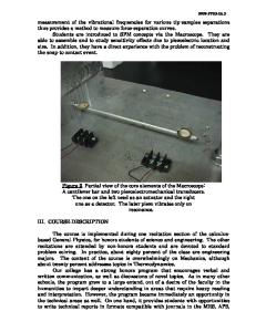
Conductive atomic force microscopy and Scanning impedance microscopy for the imaging of electrical domain in CaCu3Ti4O12 perovskite oxide Raffaella Lo Nigro, Patrick Fiorenza and Vito Raineri Istituto per la Microelettronica e Microsistemi (IMM), CNR, Strada VIII n 5, 95121 Catania, Italy. ABSTRACT Electrical characterization of CaCu3Ti4O12 (CCTO) ceramics with scanning probe based techniques has been carried out. In particular, conductive atomic force microscopy (C-AFM) and scanning impedance microscopy (SIM) have been used to demonstrate the presence, shape and size in CCTO ceramics of the different electrically domains, both at the grain boundaries and within the grains. The electrical characteristics of single grains and of single domains have been evaluated and it has been observed that the conductive grains are surrounded by insulating grain boundaries. INTRODUCTION Recently, several studies on the calcium copper titanate, CaCu3Ti4O12 (CCTO), have revealed this material to possess an impressive giant dielectric constant value of 105 times the vacuum permittivity ε0 at 1MHz, which remains constant in the 100-600 K temperature range and slightly depends on the frequency in the 102-105 Hz range [1-3]. These interesting properties render the CCTO material a real attractive alternative to the currently used ferroelectrics which in turn possess lower dielectric constant values having stronger temperature dependence. Several macroscopic and also microscopic scale investigations pointed out the possibility to explain the giant permittivity in terms of Internal Barrier Layer Capacitor (IBLC) effect [4, 5]. The IBLC effect is the widely accepted model to explain the giant permittivity phenomenon and implies the presence of conducting parts (grains) surrounded by insulating regions (grain boundaries). Most of the works in literature stated the IBLC interpretation basing their conclusions on macroscopic measurements, such as impedance spectroscopy [4]. However, the complete interpretation of the physical properties of complex oxides could take advantages by their investigation at the nanometre scale. In this context, a common feeling is that the preparation of the sample before its characterization at nanometer scale deserves great attention as well as the interpretation of the obtained data. In fact, scanning probe microscopy (SPM) techniques are very sensitive to the sample surface conditions and local phenomena, which could be the main cause of artefacts and/or erroneous data interpretation. In the present work, we report our method to avoid artefacts in nanoscopic measurements and the discrepancies among several earlier papers[5-7] will be discussed in terms of superficial artifacts affecting the SPM techniques, both from geometrical and electrical point of views. Physical considerations and criteria are given to state on the absence of misleading interpretations EXPERIMENTAL DETAILS In a rough polycrystalline surface many phenomena can be present, particularly at the grains
edges where the well-known
Data Loading...