CVD growth of Si nanocrystals on dielectric surfaces for nanocrystal floating gate memory application
- PDF / 622,911 Bytes
- 6 Pages / 612 x 792 pts (letter) Page_size
- 22 Downloads / 359 Views
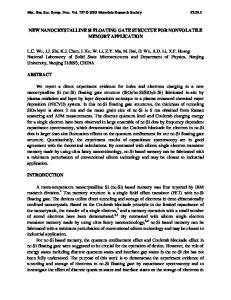
CVD growth of Si nanocrystals on dielectric surfaces for nanocrystal floating gate memory application Sucharita Madhukar, K. Smith, R. Muralidhar, D. O'Meara, M. Sadd, B-Y. Nguyen,B. White and B. Jones. Materials and Structures laboratory, Digital DNA Labs, Motorola SPS, Austin TX. Abstract Initial stages of growth of silicon on dielectric surface proceeds through Volmer-Webber growth mode (through island formation) and coalescence of islands to form a continuous thin film layer. Growth of silicon nanocrystals on dielectric surface can be achieved by controlling the nucleation and growth kinetics of these nanocrystals on the dielectric surface. In this study, we present CVD growth of Si nanocrystals on oxide, oxynitride and nitride surfaces using silane based chemistry. The effect of process conditions such as deposition temperature, precursor flow rate, carrier gas on nanocrystal incubation time, size and density of nanocrystals was studied. The nucleation and growth rate of the silicon nanocrystals is also a strong function of the surface chemistry , surface structure and strain in the dielectric film. We have studied the effect of oxide deposition temperature and surface pretreatments on the nucleation and growth characteristics of the silicon nanocrystals. Introduction Due to the continued thrust in the microelectronics industry to increase the speed and density of the devices, fabrication of nanostructures has emerged as a new forefront in Si-based technology leading to the appearance of mesoscopic and quantum devices such as single electron transistors[1], nanocrystal based floating gate memories[2] and resonant tunneling devices[3]. Amongst these devices, it is believed that the nanocrystal based floating gate memory (Figure 1) which uses a high density of nanocrystals embedded in the gate oxide to store charge on the floating gate of the MOS transistor, offers one of the most practical applications of nanotechnology. Threshold voltage of the MOS transistor can be modulated by storing or removing charge on the floating gate resulting in a binary memory operation. The threshold voltage shift is sensitive to total charge density of the floating gate and relatively insensitive to the small local spatial charge variations of the floating gate(except under extreme conditions when all the charge is stored either on the source side or the drain side of the transistor). Charge density of the floating gate is directly proportional to the areal density of nanocrystals when the average distance between nanocrystals is much smaller than the floating gate dimensions (assuming single electron storage in the nanocrystal). For successful memory sensing, the threshold voltage shift and thereby the nanocrystal density should be maximized.
Gate
Source tunnel oxide
Drain Nanocrystals
Fig.1:Schematic of a nanocrystal based memory device F5.2.1
In this study, we discuss the influence of CVD growth parameters such as precursor chemistry, carrier gases, flow rate of gas, deposition pressure, deposition temperature, deposition
Data Loading...