Deep Centers and Persistent Photoconductivity Studies in Variously Grown GaN Films
- PDF / 57,166 Bytes
- 6 Pages / 612 x 792 pts (letter) Page_size
- 81 Downloads / 273 Views
9W11.81
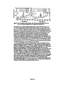
Schottky diodes with the diameter of about 1 mm, deep levels spectroscopy (DLTS) with electrical and optical injection and electron beam induced current (EBIC) profiles measurements at 300K. The latter profiles were used to extract the values of diffusion length of minority carriers. For persistent photocapacitance measurements a series of capacitance versus voltage and capacitance versus temperature (C-T) curves were measured at various frequencies before and after illumination at 85K with deuterium UV lamp and also with various light emitting diodes and with white light source equipped with selective filters. The Au Schottky diodes were prepared as described in [5]. The details of experimental set-ups and measurement procedures can be found in [5,6]. RESULTS AND DISCUSSION Table I presents the values of the (00.2) x-ray reflection halfwidths, ∆00.2, of room temperature electron concentration established from C-V measurements at 1 kHz (nC-V) and of diffusion lengths (Ld) in various n-GaN samples studied in this paper. It can be seen that the crystalline quality, as assessed by the halfwidth of the (00.2) reflection is the best for the MOCVD sample 598 grown on LT GaN buffer. The quality of the HVPE sample B95 and of the undoped MOCVD sample 385 grown using an LT AlGaN buffer is the worst in the same terms, while the undoped MOCVD LT AlGaN buffer sample 644 and lightly Si doped MOCVD LT AlGaN buffer sample 646 occupy the intermediate position. In search of centers responsible for the observed changes of Ld we first carried out DLTS with electrical injection measurements. DLTS studies on sample 385 have already been published in [6] (this is sample #1 of [6]). They showed the presence of only one dominant electron trap with apparent activation energy of 0.55 eV (the ET4 trap in the system of notation proposed in [1]). The density of these traps was found to be 2.8 .1015 cm-3. Figure 1 shows DLTS spectra measured for samples 646, B95 and 598 with time windows t1/t2=100 ms/1000 ms, with reverse bias of –0.5 V and the forward bias pulse of +1V ( the pulse duration was 2s). For sample 646 the only feature is the peak near 270K corresponding to the same ET4 trap as in sample 385. The concentration of this trap was 6.2.1015 cm-3. In sample B95, in addition to the ET4 trap with concentration 2.8.1015 cm-3, we observed an electron trap with activation energy 0.25 eV (the ET2 trap [1]) with concentration 2.5.1014 cm-3, the electron trap with activation energy of 0.8 eV (the ET6 trap [1]) with concentration of 6.4.1014 cm-3, and an electron trap with activation energy of 1 eV that is Table I. Electrical and structural properties of the studied samples Sample # 385 644 646 598 B95
Growth method MOCVD, LT AlGaN buffer MOCVD, LT AlGaN buffer MOCVD, LT AlGaN buffer MOCVD, LT GaN buffer HVPE
doping, cm-3 none
∆00.2, arcsec 540
nC-V, cm-3 2.1015
Ld, µm 0.5-0.6
none
450
5.1014
0.9-1.2
Si,
Data Loading...