Defining Conditions for the Etching of Silicon in an Inductive Coupled Plasma Reactor
- PDF / 385,270 Bytes
- 6 Pages / 412.92 x 637.2 pts Page_size
- 35 Downloads / 263 Views
ABSTRACT In high-density fluorinated plasma processes, the mechanisms that fundamentally limit the etching of silicon are poorly understood. In an effort to improve our understanding of limits to the performance of such systems, the etching of silicon wafers in an inductive coupled plasma reactor, using SF6, has been studied. A systematic empirical investigation has allowed us to define many of the experimental parameters that control the etching rate. There is little temperature dependence of etching which suggests a diffusion limited process. Systematic
variation of parameters controlling the rate of etching: total pressure in the reactor, flow rate, partial pressure of reactive species and the rf power supplied to the discharge enable us to accurately define the performance of the system. Experiments, which segregate the physical and chemical components of the etching process, support the conclusion that etching is dominated by electrically neutral species. These various results are interpreted in terms of accepted models for the reactive chemistry in plasmas containing SF 6.
The MEMS industry is placing ever greater demands on etching processes, and there is a need to achieve
the high degrees of anisotropy, and critical dimension control, at high etch-rates. The approach outlined allows us to develop effective strategies for evolving improved systems for the high rate plasma etching of silicon.
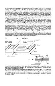
INTRODUCTION Silicon is used for micro-electro mechanical systems (M.E.M.S.), optical devices, and micro-fluidic components, and semiconductor applications. As geometries of device components get smaller, the requirement to etch silicon with vertical profiles becomes important. An increase in aspect ratio (depth to width ratio) of features is desirable because more devices can be made from the same size of silicon substrate, and also because high aspect ratio features often lead to enhanced device characteristics. In order to meet the requirements of the automotive industry, Robert Bosch GmbH originally invented a fluorine-based chemistry process which maintains verticality (anisotropy), by using the concept of alternate etch and passivation steps1 . Based on this generic approach STS have developed it's Advanced Si Etch (ASETm). The etchant gas is SF 6, and the passivant gas is C4Fg. At the beginning of each etch step, fluorocarbon polymer (deposited in the previous, passivation step) is removed from horizontal surfaces by reactive ion etching. Increased ion energy in the vertical direction results in a much higher rate of removal of fluorocarbon polymer from horizontal surfaces than from vertical surfaces. After polymer removal, the horizontal silicon surface is exposed to reactive fluorine-based species. The exposed silicon is etched during this period, whilst the vertical surfaces remain protected by the fluorocarbon polymer layer. Repeating the etch/passivation steps enables the silicon to be etched vertically by restricting the lateral etch characteristic. This technique has been developed to meet profile and d
Data Loading...