Degradation in a Molybdenum-Gate MOS Structure Caused by N + Ion Implantation for Work Function Control
- PDF / 745,746 Bytes
- 6 Pages / 612 x 792 pts (letter) Page_size
- 62 Downloads / 363 Views
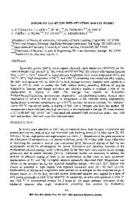
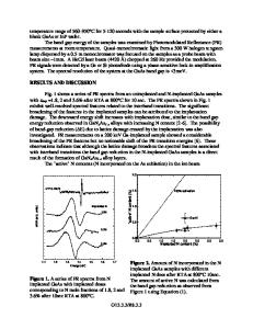
Degradation in a Molybdenum-Gate MOS Structure Caused by N+ Ion Implantation for Work Function Control Takaaki Amada, Nobuhide Maeda, and Kentaro Shibahara Research Center for Nanodevices and Systems, Hiroshima University, 1-4-2, Kagamiyama, Higashihiroshima, Hiroshima, 739-8527 Japan. Abstract An Mo gate work function control technique which uses annealing or N+ ion implantation has been reported by Ranade et al. We have fabricated Mo-gate MOS diodes, based on their report, with 5-20 nm SiO2 and found that the gate leakage current was increased as the N+ implantation dose and implantation energy were increased. Although a work function shift was observed in the C-V characteristics, a hump caused by high-density interface states was found for high-dose specimens. Nevertheless, a work function shift larger than -1V was achieved. However, nitrogen concentration at the Si surface was about 1x1020 cm-3 for the specimen with a large work function shift. Introduction The gate length of advanced CMOSFETs will be shorter than 50 nm by 2003. When that happens, a gate oxide, which is the most important factor for improving the performance of FETs, will be 1.1-1.6 nm [1]. As the gate oxide is scaled, the increase in electrical thickness due to gate depletion becomes more severe. The total loss in electrical thickness due to gate depletion and quantum effects in a channel is forecasted to be 0.8 nm. In addition, in the case of poly-Si gate CMOSFETs, the increase in gate resistance due to gate electrode thickness scaling and the boron penetration problem are serious obstacles to continuing traditional scaling. Since these problems are attributed to the necessity of doping poly-Si, a metal gate could be a potential solution Refractory metals, such as Mo, Ta, Ti, and W, and their nitrides are candidates for metal gate material. Mo especially has many advantageous features for use in the conventional LSI fabrication process. For example, Mo has a high melting point (2620oC) that is suitable for hightemperature processes like S/D activation annealing. It also has low resistivity (5.0 µΩ-cm), which is lower than that of silicide films, as well as a feature that makes it possible to apply fine patterning by the conventional dry etching process. However, conventional CMOS devices use p+-poly-Si for p-MOSFET and n+-poly-Si for n-MOSFET for threshold voltage adjustment. This means that the work function of the metal gate material must also meet this requirement. Otherwise, counter doping to the channel region, which tends to lead to mobility degradation and B7.5.1 Downloaded from https://www.cambridge.org/core. University of Arizona, on 25 Aug 2017 at 09:16:43, subject to the Cambridge Core terms of use, available at https://www.cambridge.org/core/terms. https://doi.org/10.1557/PROC-716-B7.5
an increase in fluctuation in characteristics, is necessary [2, 3]. Ranade et al. reported a work function control technique for an Mo gate [4-7]. This method uses annealing and/or N+ ion implantation. However, they did not mention the side effects
Data Loading...