Deposition of Device Quality, Low H Content a-Si:H by the Hot Wire Technique
- PDF / 321,477 Bytes
- 6 Pages / 420.48 x 639 pts Page_size
- 111 Downloads / 314 Views
DEPOSITION OF DEVICE QUALITY, WIRE TECHNIQUE
LOW H CONTENT a-Si:H BY THE HOT
A. H. Mahan, B. P. Nelson, S. Salamon, and R. S. Crandall Solar Energy Research Institute, Golden, CO 80401, USA
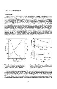
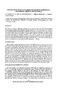
ABSTRACT We report measurements of the Urbach edge, optical bandgap, and ambipolar diffusion length on a series of hydrogenated amorphous silicon (a-Si:H) films deposited by hot-wire-assisted chemical vapor deposition (HW). We compare the properties of these films to those of a series of a-Si:H films deposited by the traditional radio frequency (rf) glow discharge (GD) technique, where we varied the substrate temperature to change the bonded H content (CH) . We show for the first time that, as CH is decreased below the value traditionally associated with device quality GD a-Si:H (-10 at.%), the electronic properties of the GD films deteriorate in the traditional manner while those for the HW samples remain device quality. Properties of these low CH HW samples will be presented and compared to those of GD films containing comparable CH. Because several indications exist that the structure of the HW films is different than that of the GD films, Raman and Small Angle XRay Scattering (SAXS) measurements are presented to illustrate structural differences. INTRODUCTION a-Si:H films have been traditionally deposited by GD decomposition of SiH4, and the technology using this deposition process has reached the point where solar cells with efficiencies >10% have been routinely deposited in many laboratories [1] . However, this deposition process does have its limitations. For example, device quality films are typically deposited at low deposition rates, and the optimum GD deposition parameters have required substrate deposition temperatures to be in a rather narrow range (200°-300*C) (1], which has been one factor in limiting the range of H content incorporated into the films. Other deposition techniques have recently been explored, in part to address some of these issues. In the present paper, we report the electronic and structural properties of a series of a-Si:H films deposited by HW deposition of SiH4. We compare the properties of these films with a series of GD deposited films, where we varied the substrate deposition temperature (TS) to vary CH in both series of films. The HW technique is not a new technique, having been used elsewhere with varying degrees of success [2,6]. However, using a certain combination of deposition parameters, we found for the first time that HW deposited, device quality a-Si:H can be deposited which contains as little as 1 at.% H. We report and contrast the electronic properties of the series of GD and Mat. Res. Soc. Symp. Proc. Vol. 219. @1991 Materials Research Society
674
HW films, particularly in the low CH (high TS) regime. Because several indications exist that the difference in electronic partially to this regime is due at least properties in structural differences, we present optical absorption, Raman, some of and SAXS data for both GD and HW films to illustrate these differences. EXPERIMENT
Data Loading...