N-Type Silicon Films Produced by Hot Wire Technique
- PDF / 1,723,198 Bytes
- 6 Pages / 612 x 792 pts (letter) Page_size
- 48 Downloads / 568 Views
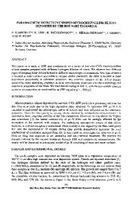
N-Type Silicon Films Produced by Hot Wire Technique Isabel M. M. Ferreira, Ana M. F. Cabrita, Elvira M. C. Fortunato and Rodrigo F. P. Martins. CENIMAT, Departamento de Ciência dos Materiais da Faculdade de Ciências e Tecnologia da Universidade Nova de Lisboa and CEMOP-UNINOVA, Quinta da Torre, 2825-114 Caparica, Portugal. ABSTRACT The role of the deposition pressure (p) and the type of filaments (tungsten, W or tantalum, Ta) used to produce large area (10cm×10cm) n-type Si:H films by hot wire chemical vapour (HW-CVD) deposition technique was investigated. The data show that the electro-optical properties of the films produced are dependent on the gas pressure used. In the pressure range of 1×10⁻³ Torr to 1.0 Torr, the room dark conductivity (σd) varies from 1×10⁻⁸ to 2 S/cm for films produced at the same hydrogen dilution and filament temperature (Tfil.). On the other hand, the hydrogen concentration (CH) decreases from 10% to 2%, while the growth rate (R) shows an exponential increase, from 1 to 9 Å/s. The SIMS analysis, within the detection limits, does not reveal the existence of any significant W or Ta contamination in the films produced. INTRODUCTION HW-CVD is a thin film semiconductor process since Wiesmen et al. [1], in 1978, used a W or C foil at temperatures around 1600 ºC to decompose silane and produce a-Si:H films. After, in 1986, H. Matsumura [2] uses a W filament instead a foil in a similar process and called it catalytic CVD. Nowadays, several groups use the HW-CVD technique [2-6] to obtain polycrystalline or amorphous silicon undoped and doped thin films. The reason for the successful of the technique is the cheap and easy way to obtain material with good electronic properties, at low substrate temperatures, suitable for device applications such as TFTs [5,6] and solar cells [5,7]. Nevertheless, to produce material with the adequate properties for device applications it requires the knowledge of the way how the deposition parameters are correlated to the electro-optical, structural and morphological properties [1,7-10]. In this work we present results concerning the influence of p and the type of filament used on R and film’s uniformity, as well as on their electrooptical and morphological properties. EXPERIMENTAL DESCRIPTION The n doped silicon films were produced by HW technique using the system depicted elsewhere [11], with Ta or W filaments. Three hot filaments 160 mm longer and 0.5 mm thick separated 25 mm from the substrate and 30 mm from each other promote the chemical decomposition of the gas. The Tfil. was measured using a QL2500 2-color digital ratio pyrometer. The gas mixture used for the process is from a pre-mixed gas bottle containing 0.7%PH3, 15.1%SiH4, 2%H2 diluted in He. For the study presented in this paper
A6.5.1
the gas process flow rate was kept at 15sccm (25.1 Pals-1), for pressures above 0.1 Torr, and of 5 sccm, for pressures below 0.1 Torr. Apart from that, the substrate temperature (Ts) was kept at 200ºC, while Tfil. was set to 1800ºC and 2000ºC, respectively for Ta and W
Data Loading...