Dielectric Properties of Ultra Dense (3 g/cm3) Silicon Nitride Deposited by Hot Wire CVD at Industrially Relevant High D
- PDF / 158,476 Bytes
- 6 Pages / 595 x 842 pts (A4) Page_size
- 32 Downloads / 237 Views
0989-A04-05
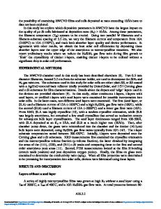
Dielectric Properties of Ultra Dense (3 g/cm3) Silicon Nitride Deposited by Hot Wire CVD at Industrially Relevant High Deposition Rates Zomer Silvester Houweling, Vasco Verlaan, Karine van der Werf, Hanno D Goldbach, and Ruud E I Schropp Surfaces, Interfaces and Devices, Utrecht University, Princetonplein 5, PO box 80.000, Utrecht, NL-3508 TA, Netherlands ABSTRACT For silicon nitride (SiNx) deposited at 3 nm/s using hot wire chemical vapor deposition (HWCVD), the mass-density reached an ultra high value of 3.0 g/cm3. Etch rates in a 16BHF solution show that the lowest etch rate occurs for films with a N/Si ratio of 1.2, the ratio where also the maximum in mass density occurs. The thus found etch rate of 7 nm/min is better than that for PECVD layers, even when made at a much lower deposition rate. The root-mean-square (rms) roughness measured on 300 nm thick SiN1.2 layers is only about 1 nm, which is advantageous for obtaining high field-effect mobility in thin-film transistors. SiN1.2 films have succesfully been tested in ìall hot wire¥¥ thin film transistors (TFTs). SiNx films with various x values in the range 1.0 < x 1.33) films [25]. I-V measurements were performed on the various MIS structures. The normalized currents (Jbreak = 10-6 A/cm2) versus the breakdown fields are shown in Figure 5. The MIS structures show no breakdown for SiNx 0 films with x ≥ 1.33 and d > 174 nm. The SiN d = 185 nm -1 SiN d = 243 nm breakdown fields obtained hence exceed 5.9 -2 -3 MV/cm. When the SiNx is too thin, shunting -4 easily occurs. For SiN1.15 no breakdown -5 -6 occurred when the nitride thickness was -7 400 nm. Other groups also report that SiNx -6.0 -5.5 -5.0 -4.5 -4.0 -3.5 -3.0 -2.5 -2.0 -1.5 -1.0 -0.5 0.0 E (MV/cm) films with higher N/Si have higher breakdown fields but also report higher Figure 5 Normalized current versus electric breakdown dielectric constants as the layers become field for two MIS structures. more N-rich [31,32], while we report a roughly constant value for the dielectric constant. Breakdown fields for PECVD or HWCVD SiNx of 2-6 MV/cm have been reported [31,33,34]. In order to meet the requirements for a good gate dielectric, the a-SiNx material has to withstand electric fields of ≥ 2 MV/cm [31]. 1.33
I / Ibreak x 10
-4
1.43
break
CONCLUSIONS Using the HWCVD method silicon nitride can be deposited possessing very low stress, which is as low as 16 MPa (tensile) for layers with N/Si = 1.1. This makes these nitrides suitable for application in MEMS. Etch rate experiments with a 16BHF solution show a minimum of 7 nm/min for SiNx films with N/Si = 1.2. At the same N/Si ratio a maximum in mass density is found, which amounts to an ultra high value of 3.0 g/cm3. Such high densities have been obtained at an industrially relevant high deposition rate of 3 nm/s. A dielectric constant of ε = 6.3 ± 0.1 and high dielectric breakdown fields exceeding 5.9 MV/cm show the potential for nitrides to be incorporated in electronic circuitry. All Hot-Wire bottom gate
staggered TFTís have successfully been
Data Loading...