Effects of Deposition Parameters on Crystallization of PECVD Amorphous Silicon Films
- PDF / 2,137,266 Bytes
- 6 Pages / 414.72 x 648 pts Page_size
- 6 Downloads / 356 Views
INTRODUCTION Polycrystalline silicon (poly-Si) films on glass substrates crystallized from amorphous silicon (a-Si) have gained significant interest for thin film transistor (TFT) applications in active matrix liquid crystal displays [1,2]. Thin film transistors fabricated in poly-Si films can be used as the pixel switching elements for the active matrix as well as the driving elements of the peripheral circuit. The poly-Si itself can be produced by direct deposition, or by laser (liquid phase) crystallization of a-Si or poly-Si precursor films, or by rapid thermal or furnace annealing (solid phase) crystallization of a-Si precursor films. In this paper we report on solid phase crystallization (SPC) of plasma-enhanced chemical vapor deposited (PECVD) a-Si films by conventional furnace annealing at 6000C in N2 ambient. We examine a-Si film crystallization and show that, upon full crystallization of the film, the grain size is influenced by deposition temperature. We correlate this to the structure of the deposited a-Si film which is observed to have a significant dependence on temperature. EXPERIMENTAL PROCEDURE
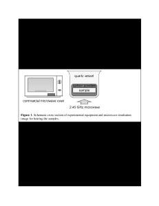
The a-Si films studied were deposited from silane (SiH 4IH2) on Corning 7059 glass substrates using a commercial PECVD reactor. Except for the substrate temperature all parameters, including gas composition and flow, were kept the same during depositions. The substrate temperature during deposition was varied between 130'C and 290'C. The deposited precursor a-Si films were characterized using spectroscopic ellipsometry (SE) measurements in order to obtain information on the structure of the a-Si film. The deposited a-Si films were then SPC annealed in N2 ambient in a conventional quartz tube furnace at 600'C for annealing times between 5 hours and 25 hours. The annealed films were characterized by means of transmission electron microscopy (TEM) using a Philips 420T microscope operated at 120 kV accelerating voltage. EXPERIMENTAL RESULTS Table I gives our SE results on the dependence of relative void density in the deposited a-Si film on substrate temperature. Here, the substrate temperature refers to the substrate temperature during a-Si film deposition. The relative void density is obtained from computer simulation of the ellipsometry data using a two-layer model. It is apparent from Table I that as the substrate temperature decreases the void density in the a-Si film increases ; as the substrate temperature is decreased from 290'C to 130TC, the void density in the film increases 0by a factor of 4. Fig.l shows TEM planar images of a-Si films deposited at 130 C and annealed at 600'C in N2 ambient for various annealing times. Large grains are observed in the film after only 5 hours of annealing (Fig. la). As the annealing time increases to 10 hours, 15 hours, and 20 hours, the grain size increases accordingly and the film reaches full crystallization after 20 hours of annealing. It 373 Mat. Res. Soc. Symp. Proc. Vol. 403 0 1996 Materials Research Society
Fig. 1 The TEM images of a-Si films deposited at 130
Data Loading...