Effects of substrates and catalysts compositions on the crystalline quality of InP Nanowires grown on SrTiO3 (001), Si (
- PDF / 5,440,718 Bytes
- 6 Pages / 595 x 842 pts (A4) Page_size
- 97 Downloads / 330 Views
1258-P04-06
Effects of substrates and catalysts compositions on the crystalline quality of InP Nanowires grown on SrTiO3 (001), Si (001) and InP (111)
K. Naji1, H. Dumont1, G. Saint-Girons1, G. Patriarche2, and M. Gendry1 1: Université de Lyon, Ecole Centrale de Lyon, INL-UMR5270/CNRS, 36 avenue Guy de Collongue, 69134 Ecully cedex, France 2 : LPN-UPR20/CNRS, Route de Nozay, 91460 Ecully cedex.
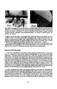
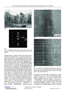
Abstract Indium phosphide (InP) nanowires (NWs) were grown by molecular beam epitaxy on various substrates including SrTiO3 (001), Si (001) and InP (111) at a growth temperature of 380°C. We used the Vapor Liquid Solid assisted method with Au as a metal catalyst. The composition of the catalyst particles and the crystalline structure of the nanowires were compared using reflection high energy electron diffraction, scanning electron microscopy and high resolution transmission electron microscope. It is found that InP nanowires grown onto InP and SrTiO3 substrates are structurally defects free with a wurtzite structure. On Si (001) substrates, the presence of stacking faults and cubic phase insertion along the growth direction is observed. The effect of the substrate on the composition of catalyst droplets and consequently on the crystalline quality of the nanowires is discussed for the conditions of nucleation and defect formation.
INTRODUCTION In recent years, the monolithic integration of III-V semiconductor on silicon has motivated a variety of research work. This integration could allow combining superior electronics properties of III V semiconductors materials with the Si technology. An additional advantage is that most of the III–V semiconductors have a direct band gap enabling systems combining micro- and opto- electronic functionalities on the same low-cost Si platform. Nanowires (NWs) grown by Vapor Liquid Solid mechanism1,2 on silicon would allow this integration without fundamental issues such as mismatch due to lattice and thermal expansion3 . However, III-V NWs grown Si (001) present two majors obstacles. First is the control of the NWs growth direction. In effect, NWs make usually a 54° angle with the substrate surface as they grow preferentially in the B direction with a wurztite structure4. It is thus difficult to obtain a vertical array of NWs on silicon (001) which is the standard choice for the electronic industry. This hampers their technological integration as light emitters. In order to favor the vertical growth orientation of NWs, we plan to use SrTiO3 (STO) oxide layer as a template on silicon according to previous results obtained by J. Cheng and al 5. They have shown that InP quantum dots could be grown onto STO (001) substrates with InP (111) planes lying parallel to the substrate surface. We expect that InP NWs on STO will adopt a
1
similar growth orientation allowing a preferential vertical growth direction. For this study we use STO substrate Second, is the question of structural defects like stacking faults, or random Wurzite/ ZincBlende phase switching of the crystal structure. Those defe
Data Loading...