Effects of the Substrate Pretreatments on the Leakage Current in the Low-Temperature Poly-Si TFTs
- PDF / 1,724,836 Bytes
- 5 Pages / 414.72 x 648 pts Page_size
- 64 Downloads / 350 Views
II. EXPERIMENTS Substrate Treatment of the Glass Substrate 1) Buffer Si0 2 Layer Formation Before the deposition of active a-Si thin films, 1000 A thickness of Si0 2 Layer was deposited directly on the Coming 7059 glass substrate in ECR CVD chamber, using SiH 4 and 02 as source gases. Alternatively, 100 A thickness of amorphous-Si film was deposited and oxidized by ECR plasma. 2) Ion Mass Doping on the glass substrate Phosphorus or Boron was doped into bare glass by Ion Mass Doping System. Source gases were PH 3 and B2H 6 diluted in hydrogen gas, respectively. The plasma power was 100W and the acceleration DC voltage was about 18KeV. PH 3 and B2H6 diluted in hydrogen were doped for 10 minutes.
419 Mat. Res. Soc. Symp. Proc. Vol. 448 ©1997 Materials Research Society
Fabrication Method of pioly-Si TFT by MILC The fabrication steps are illustrated in Fig. 1. A 1000A-thick a-Si film was deposited by LPCVD at 480 °C using pure Si 2H6, and defined for active layer. For the gate dielectric, 300A thick Si0 2 was formed by ECR plasma oxidation of active a-Si layer and then 700A thick Si0 2 was deposited by ECR PECVD using [SiH 4(25%)+Ar] gas in ECR chamber[4]. The gate and gate dielectric was patterned and defined by conventional SF 6 plasma etching and wet chemical etching (diluted BHF solution), respectively. A 20A thick Ni film was deposited without an additional mask as in Fig. l(a). Ion mass doping was carried out to form n-type gate and source/drain for n-channel TFT's. Source/drain activation and crystallization of a-Si at the channel area were done by annealing at 500'C for 15hrs. After the crystallization, unreacted Ni films on oxide area were removed by wet etching. The process conditions are summarized in table 1. Ion mass doping r-1 oxide r a-Si
Ni
(a)
substrate
(b)
Direction of MILC
so
-
A)
(c) MILC p-Si Fig. 1. Fabrication steps of MILC poly-Si TFT's. (a) Deposition of a 20 A Ni layer followed by dopant Ion Mass Doping (b) Crystallization of the source, drain and channel area (c) Metallization Process a-Si deposition gate-oxide formation gate(a-Si) source/drain doping
Method LPCVD(lOOO A, 4801C) ECR Oxidation (300 A) + ECR CVD (700 A) LPCVD (2000A, 4801C) Ion Mass doping( RF=200W, DC=I 8keV)
Ni deposition Sputtering (20 A) Al deposition Sputtering (2000 A) Table 1. Key processes for the fabrication of poly-Si TFT's by MILC.
420
III. RESULT AND DISCUSSION Metal Induced Lateral Crystallization The channel area could be crystallization by Ni deposited on source and drain area. The characteristic in Fig.2(a) indicates a-Si, which yet to be crystallized. By annealing at 500'C for 15hrs, The channel area of 40jim in length was completely crystallized as shown in Fig. 2(b). Detailed discussion of MILC phenomenon can be found in the literature[3].
(b)
(a)
Fig. 2 Nomarski optical micrographs showing the progress of MILC in the channel area. A 20 A-thick nickel layer was deposited after the source/drain definition and the width and length of the gate were 40V/40,um. a) annealing at 500 IC for I0hrs (b
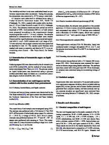
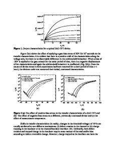
Data Loading...