Ge out-diffusion and its Effect on Electrical Properties in s-Si/SiGe Devices
- PDF / 317,371 Bytes
- 6 Pages / 612 x 792 pts (letter) Page_size
- 48 Downloads / 324 Views
0912-C02-04
Ge out-diffusion and its Effect on Electrical Properties in s-Si/SiGe Devices Suresh Uppal1, Mehdi Kanoun1, Sanatan Chattopadhyay1, Rimoon Agaiby1, Sarah H. Olsen1, Steve J. Bull2, and Anthony O'Neill1 1 School of Electrical, Electronic and Computer Engineering, University of Newcastle upon Tyne, Merz Court, Newcastle upon Tyne, NE1 7RU, United Kingdom 2 School of Chemical Engineering and Advanced Materials, University of Newcastle upon Tyne, Merz Court, Newcastle upon Tyne, NE1 7RU, United Kingdom
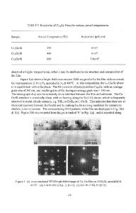
ABSTRACT In this paper we report on the quantification of Ge diffusion in strained Si/SiGe (s-Si/SiGe) structures for different Ge content in the SiGe virtual substrate. Using TCAD tools, the diffusivity has been calculated by varying pre-exponential factor and activation energy for Ge diffusion in s-Si and SiGe layers separately and obtaining a fit to the SIMS profiles. We observe an exponential and a linear dependence of pre-factor and activation energy for Ge diffusion in s-Si and SiGe, respectively, which is in agreement with literature. As a result of diffusion, the carrier confinement in thin strained layer reduces and the mobility is affected. Using C-V measurements on MOS capacitors fabricated along with devices, a shift in the flat band voltage has been observed and is attributed to a change in the interface trapped and fixed oxide charge. We observe a stronger effect of the variation of strained layer thickness than Ge content on the change in the flatband voltage. This observation is consistent with an exponential increase in Ge arriving at the interface with decrease in strained layer thickness. INTRODUCTION Hitherto, scaling of Si based CMOS devices has been the approach to fabricate faster transistors. However, straining Si in the channel region has emerged as a novel approach for achieving enhanced performance without aggressive scaling. Global or wafer level strain in Si has been achieved by growing thin layers of Si on relaxed SiGe virtual substrates (VS), generating tensile strain in Si due to its lattice mismatch with SiGe. However, the presence of Ge atoms in close proximity to the channel region leads to detrimental effects on carrier mobility [1] and the advantages of strained Si are compromised. There are three crucial factors affecting the device performance from materials perspective, namely, strained Si (s-Si) thickness, Ge content in the VS, and amount of strain in the channel. During fabrication of a MOSFET device, Ge atoms from the substrate can diffuse into the active strained layer thereby affecting the carrier mobility and interface and fixed charge density at the oxide/channel interface. In this paper we report on quantification of Ge diffusion from SiGe VS into s-Si layer and its effect on the electrical properties of the oxide in a MOS structures. EXPERIMENTAL PROCEEDURE Strained Si/SiGe NMOSFET devices and MOS capacitors were fabricated using a standard high temperature fabrication process. The Ge content in the VS was varied between 10 and 30%. Material characterisation i
Data Loading...