Electromigration Damage and Failure Distributions in Al-4wt.%Cu Interconnects
- PDF / 1,496,971 Bytes
- 6 Pages / 414.72 x 648 pts Page_size
- 77 Downloads / 513 Views
ABSTRACT Unpassivated 2.1 gm and 1.1 4tm wide lines of Al-4wt.%Cu have been electromigrationstressed to failure under accelerated testing conditions (up to 300 °C and 2 x 10¹⁰ A m-2 ). The line resistance and microstructure and the development of electromigration damage are discontinuously recorded. Distributions of damage sites (hillocks and voids) along the line lengths are measured, and the evolution of the distributions with stressing time is followed. The distances between damage sites show a clear correlation with the grain structure. Damage and failure sites are concentrated near the end of the lines at which electrons enter.
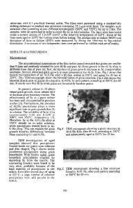
INTRODUCTION The metallization used here has been extensively studied in previous work, which has examined damage populations during testing and their correlation with median time to failure (MTF) [1,2] and electrical characteristics [3]. The populations rise linearly with testing time and the rate of increase scales inversely with the MTF [2]. The metallization in 1.1 gLm and 2.1 gm lines has a near-bamboo microstructure [3] with Al-Cu precipitates [4] which influence the development of damage and whose distribution evolves during testing [3]. The present work extends these results by examining the spatial distributions of damage and failure. EXPERIMENTAL METHODS The metallization is A1-4wt.%Cu, unpassivated, 1 jim thick, with a nominal sheet resistance of 32.5 mQ/sq., patterned and then annealed at 435 'C under nitrogen for half an hour. The lines are 1.4 mm long, with widths (estimated from resistance) of 1.1 and 2.1 gm. Each line lies between two 4.5 jim wide guard-rails of the same metallization. Lifetesting was performed at 260 and 300 'C with current densities of 2 and 1 x 10¹⁰ A m-2 respectively. Lifetests were interrupted at several times for non-destructive scanning electron microscopy (SEM) examination using both secondary and backscattered electron imaging modes. A collage was made from SEM images of the lines taken at about 3000x showing the complete 1.4 mm long test lines in a length of about 4.2 m. Every damage site (hillock or void) was registered and the positions (that is distances along the lines) recorded. The lines have a near-bamboo microstructure and at any distance along a line there is normally only at most one damage site, that is, the lines are not wide enough to accommodate two or more damage sites across the width. Therefore positions across the width were not recorded.
391
Mat. Res. Soc. Symp. Proc. Vol. 391 0 1995 Materials Research Society
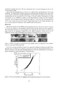
RESULTS Damage Site Distribution Along Test Lines For a 2.1 gim wide test line which was electromigration tested at 260 'C for 173 and 234 hrs, and had a resistance increase of 3 % and 24 % (i.e., failed), the distributions of damage sites along the line are shown in Figs. la and lb respectively. It can be seen in both figures that there is a concentration of damage at the cathode end of the line (that is where the electrons enter the line). At successive testing times, the damage density over the end segment of 10
Data Loading...