Stress-Voiding and Electromigration in Multilevel Interconnects
- PDF / 683,993 Bytes
- 12 Pages / 414.72 x 648 pts Page_size
- 52 Downloads / 502 Views
M.A. Korhonen, Tao Liu, D.D. Brown, and C.-Y. Li Department of Materials Science and Engineering, Cornell University, NY 14853
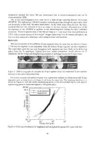
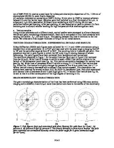
ABSTRACT Stress-voiding and electromigration have become urgent reliability concerns at the decrease of interconnect dimensions to submicron size. Severe stress voiding may arise in multilevel metallizations, particularly at contact and via regimes where the thermal stresses are highest. Via and contact structures with the attached refractory layers usually block entirely the electromigration flux; hence, EM voids are likely to form here. In this paper we first model the migration of atoms due to gradients in composition, stress, and electric potential. We seek a formulation in the spirit of irreversible thermodynamics, i.e. without reference to any specific micromechanisms of diffusion. We then apply the general developments to predict the stress evolution and void growth in Al based interconnect lines confined between entirely blocking Wstuds. We also analyze the effects of Cu depletion at vias, either by interfacial or grain boundary diffusion, on the stress evolution and void growth. Finally we demonstrate that the change in the line resistance due to void growth will display apparent incubation times even if the void grows linearly with time. INTRODUCTION Stress migration (SM) and electromigration (EM) have become urgent reliability concerns at the decrease of interconnect dimensions to submicron size. Particularly severe stress voiding problems may arise in multilevel metallizations where during processing of higher level metallizations, the stress-voids at lower level metallizations have a chance to nucleate and grow. Via and contact regimes with the attached refractory metallization layers usually block entirely the electromigration flux; here also thermally induced stresses are highest. Therefore, both SM and EM voids are likely to form at or close to the vias and contacts, being the sites of the highest stresses and the maximum flux divergence. It is generally recognized that a physically based SM and EM model is needed to assess the reliability of interconnects in service, as based on the accelerated testing data at higher temperatures and current densities. Because of the prohibitively long testing times in service conditions, the test any viable theoretical model must pass, is the simulation and prediction of SM and EM behavior observable during accelerated tests. We have previously presented the basic version of the unified physical model for SM and EM in single component metallizations [1,2] extending the original work by Blech and Herring (3]. In this paper we are concerned with extending the previous treatments to include the effect of compositional changes, particularly those due to Cu depletion during EM in Al(Cu)-based metallizations [4-7]. We then apply the general developments to predict the stress evolution and void growth in interconnect line segments confined between entirely blocking via studs. We derive equations that explicitly show the effects of current densit
Data Loading...