Electrophoretic Deposition of Carbon Nanotubes into Device Structures: An Approach to Integrate Nanostructures into Micr
- PDF / 3,953,199 Bytes
- 5 Pages / 612 x 792 pts (letter) Page_size
- 28 Downloads / 338 Views
HH13.29.1
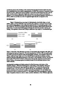
Electrophoretic Deposition of Carbon Nanotubes into Device Structures: An Approach to Integrate Nanostructures into Micro devices Madhuri Guduru, Anand Francis, Tabbetha A. Dobbins Louisiana Tech University, Institute for Micromanufacturing, P.O. Box 10137 Ruston, LA 71272-0001, U.S.A. ABSTRACT Charged particles in suspension tend to move when an electric field is applied. This simple phenomenon of migration of charged particles in a liquid medium and their subsequent deposition onto an oppositely charged electrode is called electrophoretic deposition (EPD), and is used in assembly of nanoparticles into microfabricated devices. This work reports the application of the EPD process for deposition of commercially available purified single-walled carbon nanotubes (CNT) onto microfabricated device structures. A direct current EPD in aqueous medium was used to position CNTs into two different microfabricated device structures: gold electrodes of 100nm thickness and gold microcantilevers. Control of the mass of CNTs deposited using EPD process is addressed in this work. INTRODUCTION Single-walled carbon nanotubes (CNTs) are the key materials in nanotechnology revolution. Their unique structure and properties lead to promising applications in microelectronics, including optoelectronic field emission displays and logic devices. Manipulation and assembly of single-walled carbon nanotubes into device structures is an important step toward the development of nanodevices by inexpensive means.1 Electrophoretic deposition is considered a novel approach for such assembly. Electrophoretic deposition (EPD) has been widely used in the world of advanced ceramics since its discovery in 1940 by Hamakar. More recently, EPD has received significant attention in advanced and technical ceramics because aqueous medium allows the industry to be environmental friendly.2 The EPD method is demonstrated using two microfabricated structures: gold electrodes on silicon dioxide and microcantilevers. EPD uses the mobility of particles contained in colloidal suspensions under the influence of an applied electric field in order to deposit those particles onto an electrode having opposite charge. The polarity of the CNT surface explains the direction of migration of the under an applied electric field. Electrostatic charges on the CNTs are induced by varying pH in the suspension. EPD has been used to plate nanomaterials for electronic and optoelectronic applications.3,4,5,6 A schematic of the experimental set-up used for EPD of CNTs into microfabricated device structures is shown in Figure 1. DC Voltage Supply
Electrical Connection Electrode Silicon Substrate Aqueous Suspension of CNTs
Figure 1. Schematic of electrophoretic deposition experiment.
HH13.29.2
Electrophoretic Deposition (EPD) Theory Electrophoretic Mobility, µ Electrophoretic mobility, µ, on a charged particle in dilute solutions (i.e. Ka30mV. The ζ-potential as a function of pH for CNTs used in this study is shown in Figure 3. Stable suspensions of single wall CNTs may be ga
Data Loading...