Integration of Carbon Nanotubes Devices Into Microelectronics
- PDF / 1,861,898 Bytes
- 13 Pages / 612 x 792 pts (letter) Page_size
- 71 Downloads / 428 Views
M4.5.1
Integration of Carbon Nanotubes Devices Into Microelectronics W. Hoenlein, F.Kreupl, G.S. Duesberg, A.P. Graham, M. Liebau, R. Seidel, E. Unger Infineon Technologies, Corporate Research, 81739 Munich, Germany
ABSTRACT Carbon Nanotubes (CNTs) offer extraordinary properties for applications in microelectronics. We assess the methods used to grow CNTs for integration into microelectronics, in particular, metallic carbon nanotubes for vias and interconnects as well as semiconducting CNTs for fieldeffect devices are discussed. State-of-the-art CNTFETs are compared to Si-MOSFETs. A vertical CNTFET (VCNTFET) device concept is presented which offers better growth control, adding a new quality to microelectronics and making real 3-dimensional electronics possible.
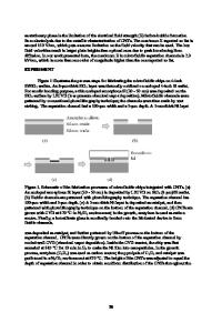
INTRODUCTION Carbon nanotubes (CNTs) display a range of exceptional properties (see Table 1) that make them promising candidates for applications in microelectronics. The ability of carbon nanotubes to form quasi-crystalline semiconducting structures with access to the bandgap and transport without scattering makes them well suited for transistor devices. The ballistic transport allows for high current densities in the metallic configurations. Moreover, multiwalled CNTs (MWCNTs) can be exploited for nanowires with many parallel, scattering free transport channels at minimum lateral space requirements and maximum length. Table 1: The most important properties of CNTs for applications in microelectronics
Electrical conductivity Energy gap
Metallic or semiconducting Eg [eV] ≈ 1/d [nm]
Ballistic, λe > 1 µm 10 Maximum current density 10 A/cm² Diameter 1-100 nm Length Up to mm 6000 W/(Km) Thermal conductivity Maximum strain 0.11% @ 1V Electrical transport
However, the silicon technology, the backbone of microelectronics, is a successful and mature technology, that relies on a number of individual processes with high yield and tremendous reproducibility. The carbon nanotube technology is still in its infancy and it has to be proven, whether it can compete with the silicon technology. On the other hand, on a longer time scale the CNT technology will benefit from new “bottom up” nanotechnology processes such as selforganization and DNA-mediated deposition. In this paper, however, we will discuss only the
Downloaded from https://www.cambridge.org/core. University of Texas Libraries, on 30 May 2020 at 23:01:51, subject to the Cambridge Core terms of use, available at https://www.cambridge.org/core/terms. https://doi.org/10.1557/PROC-772-M4.5
M4.5.2
conservative but faster approach of staying as close as possible to the silicon technology and replacing certain process modules by CNTs or even replacing silicon or copper as materials. DEPOSITION METHODS FOR CARBON NANOTUBES CNT deposition methods can be roughly divided into two basic procedures. 1. The first technique is the ex situ growth of CNTs at high temperatures (~2000 °C) by laser ablation in a furnace [1,2] or by arc discharge between carbon rods [2,3]. The yield of the furnace method can be enhanced by
Data Loading...