Fast and Controlled Integration of Carbon Nanotubes into Microstructures
- PDF / 8,229,169 Bytes
- 6 Pages / 612 x 792 pts (letter) Page_size
- 45 Downloads / 355 Views
1139-GG03-06
Fast and Controlled Integration of Carbon Nanotubes into Microstructures
Wenjun Xu1, Chang-Hyeon Ji 2, Richard Shafer2, Mark G. Allen2 1 Department of Polymer, Textile and Fiber Engineering, 2 Department of Electrical Engineering, Georgia Institute of Technology, 791 Atlantic Drive, Atlanta, GA, 30032, U.S.A.
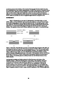
ABSTRACT In this paper, we report the results of a rapid and room temperature integration approach for the selective and structured deposition of carbon nanotubes (CNTs) into three-dimensional microstructures. The approach exploits electrophoretic deposition (EPD) from an aqueous suspension of CNTs, together with suitably patterned and electrically-energized microstructurebearing substrates. Uniform 2-D and 3-D micropatterns of CNTs on wafer scale have been achieved in less than 4 minutes with controllable thicknesses ranging from 133nm to several micrometers. Orientation of the deposited CNTs was observed in microstructures with certain dimensions. Surface hydrophobicity of the microstructures was found to be critical in achieving well-defined micropatterning of CNTs. A hydrophobic microstructure surface leads to the selective patterning profiles of CNTs, while a hydrophilic surface induces CNTs assembly over the entire microstructure, with resultant loss of selectivity. This approach can be further extended to fabricate 3-D micropatterns with multilayer materials on flexible substrate through the aid of transfer micromolding techniques.
INTRODUCTION CNTs have been intensively investigated since 1991 and exhibit promising potential in fields such as molecular electronics, microsensors, solar cells, field emission devices and biocoatings [1-5]. This high aspect ratio nanomaterial possesses interesting piezoresistive, electrical, physiochemical and mechanical properties that can serve as a key enabler in microsystems such as microsensors and microactuators [6-8]. To integrate this versatile material into miniature systems, suitable approaches are required for localizing CNTs in certain desired areas of the microstructure. In general, there are two approaches to achieve this localization: during CNT synthesis, and post-CNT synthesis. The former approach usually involves pre-patterning of catalyst at the desired sites, followed by a high temperature growth reaction. Although this approach deposits the nanotubes in a desired area directly, the high temperature required as well as the inability to refine the CNTs prior to deposition are potential limitations. The latter approach overcomes both of these limitations, at the expense of extra processing steps. There has been much previous work to pattern CNTs on substrates using a post-synthetic approach. Terranova et. al. reported assembly of CNTs across micron-sized gaps between electrodes via dielectrophoresis under AC field [9]. Cui utilized polymer-assisted self-assembly to obtain CNT layers on microstructures [10]. An AFM tip has also been used to place individual CNTs onto desired locations in nanodevices.
Good control of the thickness and morp
Data Loading...


