Integration Of Carbon Nanotubes Into Device Structures
- PDF / 2,095,414 Bytes
- 6 Pages / 612 x 792 pts (letter) Page_size
- 84 Downloads / 444 Views
HH13.3.1
Integration Of Carbon Nanotubes Into Device Structures B. Lägel, J.D. Schumacher, N. Nguyen, B. Zivanovic and R. Schlaf Department of Electrical Engineering, University of South Florida, Tampa, Fl 33620 ** To whom correspondence should be addressed: email: [email protected]
ABSTRACT Carbon nanotubes have shown promising properties for applications in electronic circuits and other device structures. Several device structures have been demonstrated in recent years by manual manipulation of single nanotubes. The integration of large numbers of nanotubes on wafer size substrates, however, has been a challenge. Our approach addressing this issue utilizes nano-patterning methods in combination with plasma enhanced chemical vapor deposition to directly assemble carbon nanotubes on wafer structures. A secondary formation step is used to actually form device structures connecting the nanotubes to electrode structures. We present first results demonstrating the feasibility of our approach. Electrode structures were prepared using multi-step electron beam lithography processes. Carbon nanotubes were grown in pre-defined locations, and contact formation procedures were carried out to establish multi-terminal contact structures.
INTRODUCTION Carbon nanotubes (CNTs) exhibit unique electrical and mechanical properties that make them ideal for applications e.g. in electronics, displays or sensors [1]. While the first CNT-based transistor working at room temperature was reported already in 1998 by Dekker [2], the integration of large numbers of nanotubes on wafer size substrates for batch production of CNTbased devices has been a challenge. This is mainly due to the lack of control not only over the properties of the CNTs but also their assembly as pointed out by Busnaina in a recent review [3]. So far, CNT-based device structures have been demonstrated mainly by spreading CNTs dispersed in solution onto a substrate, resulting in randomly distributed nanotubes [4, 5]. In this paper we report our approach to integrate carbon nanotubes into device structures by direct assembly of CNTs on a patterned substrate via catalyst-mediated plasma enhanced chemical vapor deposition (PECVD). First, we demonstrate the growth of precisely positioned aligned CNT arrays from Ni dots in holes etched into SiO2 on a Si substrate. For the manufacture of CNT-based devices, we prepared contact electrode structures on thermally oxidized Si substrate wafers via conventional photolithography. A second set of smaller electrodes with Ni catalyst patterns was then fabricated by electron beam lithography and e-beam evaporation before individual freestanding CNTs were grown at the end of one of the electrodes.
HH13.3.2
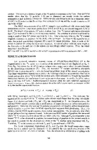
EXPERIMENTAL 1) Substrate Patterning a) CNT Arrays In order to investigate and demonstrate selective growth of aligned carbon nanotubes from patterned catalyst films we have fabricated dot array patterns on thermally oxidized p-type Si(111) substrates via electron beam lithography, see fig. 1. The oxide layer on the Si substrate has
Data Loading...