Etching and Charging Effects on Dose in Plasma Immersion Ion Implantation
- PDF / 228,719 Bytes
- 6 Pages / 414.72 x 648 pts Page_size
- 100 Downloads / 293 Views
JIQUN SHAO Eaton Corporation, Semiconductor Equipment Division, 108 Cherry Hill Drive, Beverly, MA 01915
SHU QIN, ZHUOFAN ZHAO AND CHUNG CHAN Plasma Science and Microelectronics Laboratory, Department of Electrical and Computer Engineering, Northeastern University, Boston, MA 02115
ABSTRACT
A general relation between the implanted dose and the processing time for plasma immersion ion
implantation (PIll) can be established through the dynamic sheath model. In practice, etching and charging effects have to be taken into account in PHI dose estimation.
Plasma immersion ion implantation (PIlI) has been tested in fabrication of semiconductor devices with shallow junctions and in hydrogenation of poly-Si thin film transistors (TFT). PHI doping is more suitable than conventional implantation for such applications because of its high
dose rate at lower energy. Since the dose rate in PIH does not depend on the area being treated, the effective current will be higher if a larger implanted area is involved. However, the relation
between dose and time is not always straightforward. During PHI processing possible etching and charging will affect the total accumulated doses. This paper presents a model for each which allows a proper compensation to be performed.
BASIC MODEL The collisionless dynamic sheath model [11 [2] for PIII can be expressed by a ChildLangmuir law and uncovering of the sheath edge during sheath expansion, so that
2qV3/2 49'IN 111 Mat. Res. Soc. Symp. Proc. Vol. 354 0 1995 Materials Research Society
(1)
and
S= qn" ds(2 -d
(2)
wherej is the ion current density, so is the free-space permittivity, q is the ion charge, M is the ion mass, V, is the absolute value of the pulse potential, n, is the ion density, and s is the sheath thickness. The sheath expansion versus the time s(t) can be obtained by solving the Eqs. (1) and (2). After the dynamic sheath is established, the total ion current density during the high voltage pulse can be directly derived from the Child-Langmuir law plus a so-called displacement current [3] [4], so that 4 j,(t)-=2
(3)
1
or
S(t)9
M
s(t) 4
J'
where so is the initial ion-matrix sheath thickness. The implant ion dose during a pulse can be obtained by integrating ion current density through pulse width as follows
dose =q" j! (t)dt.
(4)
q
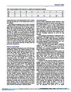
ETCHING EFFECT ON DOSE With the fabrication of PMOS using PIII technology, BF 3 gas has been used as the boron dopant source due to its low toxicity relative to B2H6 . Not only are ions implanted, but because of the fluorine ions there may be both etching or deposition at the Si wafer surface. Some of the implanted boron ions would be lost with the etching. Therefore, the retained dose is less than the incident dose estimated from Eq. (4). In general, during reactive material PIII, the surface etching must be considered in the dose control of the process. In our previous work [5] the BF 3 PIII etching rate of silicon and SiO 2 is measured under well-controlled conditions and a dose-time relation is derived through a computer simu
Data Loading...