Evolution of nucleation sites and bubble precursors in silicon as a function of helium implanted dose
- PDF / 498,915 Bytes
- 6 Pages / 595 x 842 pts (A4) Page_size
- 62 Downloads / 541 Views
Evolution of nucleation sites and bubble precursors in silicon as a function of helium implanted dose Changlong Liu1, R. Delamare1, E. Ntsoenzok1, G. Regula2, B. Pichaud2, A.Van Veen3 1 CERI-CNRS, 3A Rue de la Férollerie, 45071 Orléans CEDEX, France 2 UMR TECSEN, University of Marseille – Faculté des Sciences et Techniques 231, 13397 Marseille CEDEX 20, France 3 IRI, Delf University of Technology, Delf, The Netherlands
Abstract
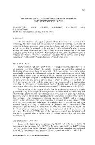
(111) oriented silicon samples were implanted at room temperature with 1.55 MeV 3He ions in the dose range of 5×10¹⁵ to 5×10¹⁶/cm2. Cross-sectional transmission electron microscopy (XTEM) was used to study the evolution of bubbles and extended defects during subsequent thermal annealing at 800°C and 900°C for 30min. The He desorption from bubbles and bubble precursors was measured by means of nuclear reaction analysis (NRA). TEM observations show that no bubbles were observed in Si implanted at doses lower than 1×10¹⁶/cm2, while a well-defined cavity band was formed after implantation at 5×10¹⁶/cm2 and subsequent thermal annealing. At the intermediary dose of 2×10¹⁶/cm2, however, the evolution of bubbles and extended defects is quite different. The bubbles prefer to nucleate in large planar clusters surrounded by a high density of dislocation loops emerging from them. The clusters of bubbles act as the sources of the dislocation loops. NRA measurements indicate that the He desorption behavior is also dose-dependent. The He desorption is achieved much faster in low dose implanted Si. The results are qualitatively discussed.
1. Introduction In the last ten years, high dose helium implantation into silicon has received considerable attention due to the formation of nanocavities and the interesting properties of such structures. Nanocavities have been demonstrated to be efficient sites for gettering fast diffusing metals [1-2]. Potentially, this gettering procedure can be used to remove metallic impurities from the active device region. Moreover, nanocavities introduce deep levels in the silicon band gap, and thus, this property can be used to control the carrier lifetime in silicon devices[3-4]. The formation of nanocavities in silicon was first observed by Griffioen et al. [5] in 1987. In this case a silicon sample was subjected to 10keV He implantation at a dose of 2×10¹⁷/cm2 followed by subsequent annealing at 1275K. Since that time, many experiments have been performed to study the main features of the cavity formation. It has been found that the nucleation and growth of He cavities in Si depend on many parameters, such as, ion dose, ion energy, ion flux, implantation temperature, impurities, etc. [6-7]. Indeed, the cavity formation in He implanted silicon is a quite complex phenomenon and involves the sequence of several mechanisms. Therefore, up to now, a clear picture on the nucleation and growth of cavities has not yet been obtained. MeV He implantation gives the opportunity to produce cavities in the bulk far beyond the surface. In this case, the effects of the surface are expected t
Data Loading...