Fabrication of GaN mesa structures
- PDF / 408,797 Bytes
- 7 Pages / 612 x 792 pts (letter) Page_size
- 37 Downloads / 375 Views
Internet Journal of Nitride Semiconductor Research:
Email alerts: Click here Subscriptions: Click here Commercial reprints: Click here Terms of use : Click here
Fabrication of GaN mesa structures K.V. Vassilevski, M.G. Rastegaeva, A.I. Babanin, I.P. Nikitina and V.A. Dmitriev MRS Internet Journal of Nitride Semiconductor Research / Volume 1 / January 1996 DOI: 10.1557/S1092578300002106, Published online: 13 June 2014
Link to this article: http://journals.cambridge.org/abstract_S1092578300002106 How to cite this article: K.V. Vassilevski, M.G. Rastegaeva, A.I. Babanin, I.P. Nikitina and V.A. Dmitriev (1996). Fabrication of GaN mesa structures. MRS Internet Journal of Nitride Semiconductor Research, 1, pp e38 doi:10.1557/S1092578300002106 Request Permissions : Click here
Downloaded from http://journals.cambridge.org/MIJ, IP address: 128.210.126.199 on 27 Jun 2016
M R S
Internet Journal o f
Nitride S emiconductor Research
Volume 1, Article 38
Fabrication of GaN mesa structures K.V. Vassilevski Cree Research EED M.G. Rastegaeva Ioffe Physical-Technical Institute A.I. Babanin, I.P. Nikitina, V.A. Dmitriev Cree Research EED and Ioffe Physical-Technical Institute This article was received on May 31, 1996 and accepted on November 22, 1996.
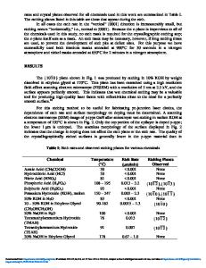
Abstract We report on nickel based technology for the fabrication of GaN mesa structures. Ti/Ni ohmic contacts for n-doped GaN with contact resistivity Rc ~2×10⁻⁵ Ω ×cm2 and Ni ohmic contacts for p-doped GaN with Rc ~ 4×10⁻² Ω ×cm2 were formed. Both types of contacts were used as masks for GaN reactive ion etching (RIE) in a CCl2F2/Ar gas mixture. Maximum etch rates of ~ 40 nm/min were obtained. Mesa structures up to 3 µm in height were formed.
1. Introduction GaN and related Al(In)x Ga1-xN solid solutions are wide band gap materials which are promising for a variety of applications such as laser diodes [1], light emitting diodes [2], microwave and high temperature devices [3] [4]. To realize the great potential of III-V nitrides and to follow the recent progress in their epitaxial growth, especially by MOCVD [5] and HVPE [6], it is necessary to develop the appropriate post-growth device fabrication technologies. Among other problems, the formation of ohmic contacts for n- and p-doped materials and RIE process are of the greatest importance. An additional requirement for these technological stages is their mutual compatibility in the process of device fabrication. The goal of this research was to find a metallization suitable for self-aligned technology so the ohmic contact could be used as a mask for GaN RIE. or so that the mask could be used as a contact. Various metals have already been used to form contacts to GaN. Ti, Ti/Al and TiN [7] [8] [9] [10] were utilized for n-GaN. TiN, Au, Au/Mg [8] , Cr/Au [11] and Ni/Au [12] were used for p-GaN. We investigated Ni-based contacts, since Ni can be used as a mask for GaN plasma etching [13], and as a Schottky barrier to n-GaN [14]. In addition, Ni is usually used to form an ohmic contact to 6H-SiC, which is a highly suitable subs
Data Loading...