Fabrication of Micro-Relief Structures in Thick Resist for Anti-Counterfeiting Applications
- PDF / 2,563,495 Bytes
- 6 Pages / 612 x 792 pts (letter) Page_size
- 105 Downloads / 276 Views
J4.4.1
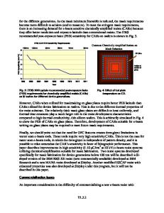
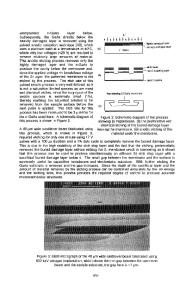
Fabrication of Micro-Relief Structures in Thick Resist for Anti-Counterfeiting Applications Patrick W. Leech1 and Henning Zeidler2, 1 CSIRO Manufacturing and Infrastructure Technology, Melbourne, AUSTRALIA. 2 Chemnitz Technical University, Chemnitz, GERMANY. ABSTRACT Micro-relief surfaces including grating structures, greytone/micrographic features and microramps have been fabricated with depth features of up to 30 µm. Grey scale lithography has been used to produce the microstructures by a single UV exposure into a layer of thick resist. Arrays of the pixelated microstructures have formed the security features on the surface of optically variable devices. Each of the microstructures was designed to provide an intended optical effect in features such as portraits, symbols and lettering which comprised a larger image (typically 2.5 x 3 cm). An essential part of the process has been the determination of the optimum conditions for coating of the thick resist (AZ P4620) as a function of spin speed and exposure. INTRODUCTION Grey-tone lithography has become an established method of forming contoured, threedimensional (3D) microstructures. Also known as relief micromachining, this technique has typically used UV exposure through a variable-transmission mask to fabricate topographic profiles in thick resist. The greyscale levels within the mask have been defined by either modulation in the size of the transparent pixels on an opaque chrome background [1] or by varying optical density in high energy beam sensitive glass [2]. Prominent applications of greytone lithography have included the fabrication of arrays of reflective/ diffractive optical elements [3] and microlenses [4]. In this paper, we introduce another application of relief micromachining in anticounterfeiting devices for financial transaction documents. The incidence of counterfeiting of banknotes, checks and authentication documents has increased significantly in recent years [5]. As an effective means of countering this trend, the use of optically variable devices embossed into foil has become widespread. These devices have proven extremely difficult to counterfeit because of the complex pattern of fine tracks and the requirement of an advanced technology such as e-beam lithography in order to produce the image [6,7]. However, the incorporation of a diffractive foil in security documents has also required an additional manufacturing process. As an alternative to security foils, we have developed a novel form of 3D relief structure intended for the direct printing of specialized inks and laquers onto a document. The relief microstructures were designed with a typical depth dimension of 15-30 µm to accommodate the variation in surface profile of the paper due to unevenness in the distribution of fibres. The master image formed in resist has been generally copied into nickel by electroplating in order to provide a durable mold for the printing of the pattern on the inked substrate surface. The resulting imprinted devices have been designed to provide a me
Data Loading...


