The Fabrication of Complex Membrane Structures in N-GaAs for Micromechanical Applications
- PDF / 2,721,220 Bytes
- 6 Pages / 414.72 x 648 pts Page_size
- 36 Downloads / 286 Views
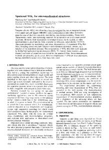
630 keY or 4 MeV with the sample held at room temperature; the projected range of these ions was predicted using the TRIM program [7] to be 0.85 Im and 3.1 pIm respectively. The damage and implanted ion profiles produced by the implantation of both 630 keV and 4 MeV nitrogen ions in GaAs, which are simulated using TRIM, are shown in Figure 1. The doses used here were 2 x 101, cm-2 for 630 keV implants and 1 x 1015 cm- 2 for the 4 MeV implants since, according to TRIM simulations, they produced almost identical damage concentrations at the sample surface, see Figure 1. In the case of both ion energies, the optimum annealing conditions were a temperature of 600 0C for ten minutes in flowing hydrogen. The structure and surface quality of the fabricated membranes were studied using a scanning electron microscopy (SEM). 3
3
0
4 MeV
0 2 ..
----.
2 E3
0r-
t 0
U "
630 keV
0
0
0
2
1
3
4
Depth (pm) Figure 1: TRIM simulations of the concentration of vacancies and nitrogen in GaAs after implantation of nitrogen using energies of 630 keV and 4 MeV with doses of 2 x 10¹⁴ and 1 x 101 cm° 2 respectively at room temperature. BASIC MEMBRANE FABRICATION PROCESS This process uses the implantation of nitrogen to compensate resistivity layer. Nitrogen is used here as it efficiently compensates projected range for the definition of the membrane thickness structures. The high resistivity of this layer is then used to protect anodic etching of the material.
n-GaAs and to produce a high the Si doping, has an appropriate and produces thermally stable it from etching during the pulsed
TRIM simulations of the implantation of energetic nitrogen ions into GaAs produces a buried highly damaged layer whose depth is determined by the ion energy and the extent of the damage is determined by the ion dose. Between this highly damaged layer and the sample surface is a thick lightly damaged layer. The samples are passivated with a 200 nm thick layer of Si3N4 which is deposited at a temperature of 3000C using plasma enhanced chemical vapour deposition; this layer is used to prevent As outdiffusion during annealing. After annealing the samples at 6000 C for ten minutes in an optical rapid thermal annealing system in an atmosphere of flowing hydrogen, the lightly damaged surface layer is compensated by the implanted nitrogen [8] and becomes semi-insulating (SI) with a high resistivity, the value of which depends on the nitrogen ion dose used. In contrast, the damage in the heavily damaged layer is only partially removed during this low temperature annealing process. Similar results for the annealing induced damage recovery have been obtained previously for MeV oxygen implantation into GaAs [9]. A Au-Ge-Ni ohmic contact, which is annealed at 450 0C for thirty seconds, is prepared on the back surface of the sample to provide an electrical contact to the GaAs during pulsed anodic etching. The membrane pattern is then defined photolithography on the sample surface. Wet chemical etching using a solution comprising H3PO 4:H20 2:methanol in the
Data Loading...