Fabrication of Si-Ge Compound Nanowires by the FZ Melting Vapor Method
- PDF / 1,909,874 Bytes
- 6 Pages / 612 x 792 pts (letter) Page_size
- 34 Downloads / 282 Views
F3.31.1
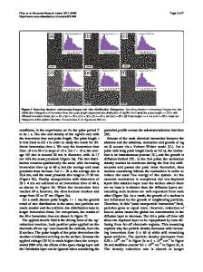
Fabrication of Si-Ge Compound Nanowires by the FZ Melting Vapor Method Quanli HU 1, Hiroshi ARAKI, Hiroshi SUZUKI, Nobuhiro ISHIKAWA, Wen YANG and Tetsuji NODA National Institute for Materials Science, 1-2-1 Sengen, Tsukuba, Ibaraki 305-0047, Japan ABSTRACT A simple method, floating zone melting vapor, was used for fabricating nanowires of Si-Ge material. Single-crystalline nanowires were successfully synthesized. TEM images of these nanowires indicated that each nanowire consists of an inner single-crystalline core and an outer layer. An observation using high-resolution transmission electron microscopy (HRTEM) showed that almost all nanowires have a similar growth orientation to the crystalline core: [210]. The coexistence of germanium-self-catalyzed and oxide-assisted mechanisms has also been suggested. INTRODUCTION Nanowires of semiconductor material are of interest in science and engineering [1][2]. Due to their high-surface area and low dimensionality, many new physical properties, such as thermal physics, optical electronics, and quantum confinement, are expected [3]. Therefore, they are certainly important components for the future applications of nanoscale devices. The challenge for finding the nanowires of semiconductor materials that can be used as building blocks with various characteristics is necessary for bottom-up engineering in the field of non–pure-silicon technology. Compared with pure silicon material, Si1-xGex is a new system that will allow band-gap engineered devices with higher performance or new functionality [4] because Si-enriched Si-Ge alloys have greater carrier mobility of electrons and holes. Growth technologies used to fabricate nanoscale Si1-xGex films include primarily molecular beam epitaxy (MBE) and ultrahigh vacuum chemical vapor deposition (UHV/CVD) [5]. However, the fabrication of alloy Si-Ge nanowires with a crystalline structure is less challenging. Moreover, primarily, [112] or [110] was the reported growth direction of silicon nanowires that was obtained by using the thermal evaporation method, and a related model was suggested. No other growth direction was found. In the present work, the nanowires of the Si-Ge alloy have been successfully synthesized, and a special growth direction resulting from different growth mechanisms has been found.
F3.31.2
EXPERIMENTAL DETAILS Silicon and germanium bulk (purity: 99.999 at %) were weighted and mixed according to the chemical ratio Si:Ge= 80:20. The mixture was melted by an arc-melting furnace in vacuum. The ingot was ground into powders (particle size: 300 mesh). And the powders were placed into a rubber tube (diameter: 8 mm; length: 70-100 mm) to be shaped into a bar with a hydraulic press at a pressure of 170 MPa. The bar of raw material was pre-sintered in a vacuum (1.33 x 10⁻⁵ Pa) at 1173 K for 2 h. Then the sintered bar was melted using the floating-zone (FZ) method inside a quartz tube at 1673 K to fabricate silicon-germanium nanowires under an atmosphere of pure flowing argon (>10 cm3 /min). The floating melting
Data Loading...