Field Emission Structure with Shottky-Barrier Electrode
- PDF / 60,834 Bytes
- 5 Pages / 612 x 792 pts (letter) Page_size
- 28 Downloads / 324 Views
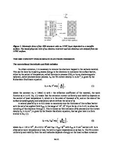
Field Emission Structure with Shottky-Barrier Electrode Andrey P. Genelev, Alexey A. Levitsky1, Vladimir S. Zasemkov Krasnoyarsk State Technical Univ., Vacuum Microelectronics Lab., Krasnoyarsk, RUSSIA 1 Krasnoyarsk State Technical Univ., Dept. of Radioelectronics, Krasnoyarsk, RUSSIA ABSTRACT We analyze a non-traditional version of semiconductor field emission structure, based on silicon cones arrays and destined for application in low-voltage vacuum microelectronics devices. In proposed construction, the gate electrode is used as Shottky-barrier contact on silicon tips. Due to Shottkybarrier contact we have obtained depletion layer in tip body under the gate electrode. Therefore variation of the gate electric potential provides the emitter current modulation. Experimental structures were fabricated with about 28000 silicon cones per 1 mm2 by reactive ion etching through a silica mask. Using a quasi two-dimensional model, we have computed these emitter structures. The model takes into account non-uniformity of silicon cone cross-section. Here, we study the influence of emitter tips parameters on the structure performance. Initial results prove the possibility of cathode current electric control with the gate electrode potential. Additionally we have obtained some other electric parameters of the emitter with the Shottky-barrier contact. The results of numerical analysis and experimental study provide a guide for design of proposed field emitter structure. INTRODUCTION One of practice problems in vacuum microelectronics is to decrease voltage operation of fieldemission devices [1,2]. Low-voltage operation can yield functional integration of semiconductor and vacuum devices. Therefore low-voltage is a goal for great variety of vacuum microelectronics applications. We have investigated a field-emission device with the gate electrode, which was formed as the Shottky barrier contact on the cathode electrode surface. Fig.1 illustrates schematically a crosssection of the emitter cone with the metal gate. MODELING Our goal now is to research the metal gate control. To achieve this goal we have studied the gate electric bias and carrier density influence on the depletion layer thickness in emitter body under the gate. When computing we were based on the traditional assumptions for the field-effect transistor model [3]. Figure 2 shows the model of the semiconductor emitter with the metal gate. The basic equations for current in the emitter cone are Poisson’s equation and the current continuity equation. Because of nonuniform geometry of the cathode tip we use modified forms
R5.6.1
of Poisson’s equation [4,5]. Equation for electric current density j(x,t) includes the dynamic component for the external circuit.
Silicon microtip Metal gate Insulator
Figure 1. Cross-section of emitter cone with metal gate.
Gate
0 Figure 2. Structure of the computed silicon cone with the metal gate. Therefore this equations for n-type semiconductor are expressed as follows:
∂Ex ( x, t ) 1 ∂S( x) q + ⋅ Ex ( x, t ) = [n( x, t ) − N0 ( x)] ,
Data Loading...