Formation of Ge Nanocrystals in High-k Dielectric Layers for Memory Applications
- PDF / 735,247 Bytes
- 6 Pages / 612 x 792 pts (letter) Page_size
- 54 Downloads / 389 Views
1250-G06-04
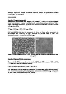
Formation of Ge Nanocrystals in High-k Dielectric Layers for Memory Applications P. Dimitrakis1, V. Ioannou-Sougleridis1, P. Normand1, C. Bonafos2, S. Schamm-Chardon2, A. Mouti2, B. Schmidt3, J. Becker4 1 Institute of Microelectronics, NCSR “Demokritos”, 15310Aghia Paraskevi, Greece 2 CEMES-CNRS, Universite de Toulouse, nMat group, BP 94347, 31055 Toulouse cedex 4, France 3 Research Center Dresden-Rossendorf, Dresden, Germany 4 Cambridge Nanotech Inc, Cambridge, MA, USA ABSTRACT This paper reports on the fabrication of Ge-NCs in Al2O3 and HfO2 layers by ion-beamsynthesis for memory applications. After furnace annealing at 800°C, Ge-NCs form in Al2O3 materials as revealed by TEM and EELS investigations, while no signature of such NCs is observed in the HfO2 layers. The charge storage properties of the non- and Ge-implanted Al2O3 layers were examined as a function of the annealing temperature in the 700-1050°C range using MIS capacitors. Strong charge storage is detected in the 800-950°C-annealed and Ge-implanted Al2O3 layers leading to large and similar memory windows. The I-V characteristics of SiO2capped Ge-implanted-HfO2 structures exhibit significant negative-differential-resistance effects probably due to the formation of conductive paths made of hafnium germanide (HfGe2) or hafnium germanate (HfGeO) regions. INTRODUCTION Semiconductor nanocrystals (NCs) have been employed successfully in various demonstrators for new CMOS device applications like nonvolatile memory (NVM) cells [1] and optoelectronic components [2]. Ge nanocrystals are of special interest for nano-floating gate NVM cells due to their band offsets with respect to the bands of the Si substrate; an attractive NC property for faster programming speeds and longer retention times compared to silicon NCs [3]. Another interesting option is the use of high-k materials as tunneling and blocking dielectrics. High-k materials offer the advantages (1) to prevent the back tunneling of trapped charges through the use of thick tunneling layers and (2) to increase the coupling coefficient between the control gate and the nano-floating gate when they are employed as blocking dielectrics [4]. Furthermore, at retention mode the internal electric caused by trapped charges is significantly lower precluding the charge loss due to tunneling through the injection and control oxide layers. This route has been examined to overcome the charge retention issues rising from the thinning of the injection SiO2 layer. Based on the above, Ge-NCs embedded in high-k dielectrics provide a promising alternative in the development of NC-memories. This work examines the prospect of using the low-energy ion-beam-synthesis (LE-IBS) technique for fabricating Ge-nanocrystals in thin Al2O3 and HfO2 layers. This CMOS compatible and timeproven technique has been successfully employed the last ten years in the formation of Si [5] and Ge [3] nanocrystals in thin SiO2 films. Structural and electrical characterization of non-implanted and Ge+-implanted Al2O3 and HfO2 layers are herei
Data Loading...