High-performance detectors for visible near-IR imaging sensors developed
- PDF / 451,611 Bytes
- 2 Pages / 585 x 783 pts Page_size
- 97 Downloads / 332 Views
High-performance detectors for visible near-IR imaging sensors developed The pitch There is significant interest in developing low-cost visible infrared (IR) sensors for a variety of applications such as imaging sensors for defense, homeland security, and commercial applications (Figure 1). There are several other technologies such as indium gallium arsenide (InGaAs), indium antimonide (InSb), and mercury cadmium telluride (HgCdTe) that cover different parts of the IR spectrum. HgCdTe IR focal-plane arrays are being developed for 3–5 μm and 8–14 μm applications. InSb is being used for 3–5 μm applications. Similarly InGaAs offers an attractive approach for visible near-IR sensors that can cover spectral bandwidths up to 1.8 μm. Silicon germanium (SiGe) offers a low-cost alternative for developing visible near-IR sensors that will not require any cooling and can operate from 0.4 μm to 1.6 μm. In addition, there are new approaches that can further increase the spectral sensitivity to 2 μm and beyond. This technology has the potential for a small unit cell size and can be built with megapixel visible near-IR cameras. The characteristics that make IR sensors appropriate for defense applications also benefit many industrial and
scientific applications. Several applications for environmental monitoring and control use IR sensors. For example, low-cost IR-based systems can be used for night vision for vehicles, for robot vision, and for medical thermography for cancer and tumor detection during diagnosis and surgery. With higher volume and lower cost these sensors and cameras will also be used in cell phones for a variety of defense and commercial applications. The market for these sensors is projected to grow over the next decade.
The technology
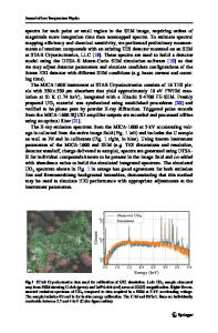
Figure 2. A cross-sectional schematic of a Ge-on-Si photoSiGe-based visible-IR diode for a visible near-infrared photodiode. arrays offer a low-cost alternative for developing near-IR sensors that will not require the integration process using both VOxany cooling and can operate in the visbased microbolometers and amorphous ible and near-IR (VIS-NIR) bands. To silicon-based microbolometer arrays that efficiently access the VIS-NIR band for are sensitive in the 8–14 μm region for various applications, high-Ge-content thermal imaging applications. Bolomlayers are required. Magnolia Optical eters convert the IR signal into change Technologies’ SiGe pin (large intrinsic of resistance that is detected. region sandwiched between p-doped and n-doped semiconductor regions) photodiodes are fabricated with 1.7-μm thick Ge layers grown directly on 15 cm Si substrates, using low-pressure chemical vapor deposition in an epitaxial growth system. After Ge growth, standard complementary metal oxide Opportunities semiconductor processes Magnolia Optical Technologies is are used to deposit and patdeveloping SiGe-based imaging sensors for tern a dielectric film to open defense and commercial applications. We are exploring potential applications and teaming windows to the Ge surface. with commerci
Data Loading...


