High Performance IGZO TFTs with Modified Etch Stop Structure on Glass Substrates
- PDF / 317,426 Bytes
- 6 Pages / 432 x 648 pts Page_size
- 9 Downloads / 327 Views
High Performance IGZO TFTs with Modified Etch Stop Structure on Glass Substrates Forough Mahmoudabadi1, Ta-Ko Chuang2, Jerry Ho Kung3, and Miltiadis K. Hatalis1 1
Display Research Laboratory, Lehigh University, Bethlehem, PA 18015, USA Corning Incorporated, Corning, NY 14831, USA 3 Department of Electro Optical Engineering, National United University, Miaoli 36003, Taiwan 2
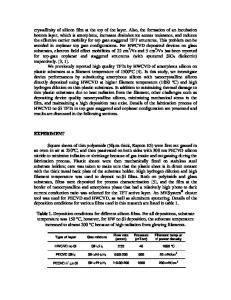
ABSTRACT In this paper, we present fabrication and characterization of RF sputtered a-IGZO TFTs having a modified etch stopper structure with source/drain contact windows on glass wafers. The effect of annealing time and channel length on device performance in terms of mobility, on/off current ratio, average off current, threshold voltage, and sub threshold slope is reported. INTRODUCTION Amorphous oxide semiconductors and in particular, amorphous indium-gallium-zinc oxide (a-IGZO) thin films are gaining considerable interest for display and flexible electronics applications. At present, thin film transistor technologies based on hydrogenated amorphous silicon (a-Si:H) and polycrystalline silicon (poly-Si) are widely utilized in production of flat panel displays. However, the low mobility in a-Si:H TFTs limits their applications in large high resolution displays. Poor stability of a-Si:H TFTs also limits their use in AMOLED display applications. The cost of the poly-Si TFT is considered to be relatively high. Furthermore, the grain boundaries present within poly-Si deteriorates device performance uniformity. These are some reasons for the ever increasing interest for developing metal oxide semiconductors like aIGZO TFTs. Studies have shown that a-IGZO are superior to a-Si:H and organic semiconductors in terms of stability. Other reported advantages of amorphous metal oxides such as a-IGZO include good uniformity, high mobility, and feasibility of room temperature processing; these advantages make them good alternatives to both silicon based and organic semiconductors for display and other large area electronic applications [1-3]. This paper reports on characteristics of a-IGZO TFTs having a modified etch stop structure and investigates the effect of channel length on TFT performance. The bottom gate TFTs in this study are fabricated on glass substrates. EXPERIMENTAL Figure 1 shows a photograph and a cross sectional view of the TFT structure. The bottom-gate TFTs were fabricated by first depositing 140 nm of Aluminum doped with Nd (AlNd) onto 150 mm Corning LOTUS glass substrates and patterning the aluminum film by liftoff in order to form gate electrodes. A 120-nm-thick SiO2 layer was then deposited by PECVD to serve as the gate dielectric. RF sputtered 50 nm of IGZO thin film formed the active layer of the TFTs. Deposition was done at 150 W from a 150 mm target in an argon/oxygen ambient at a deposition pressure of 6 mtorr. A 50 nm RF-sputtered SiO2 film served as the first passivation layer (active passivation layer shown in Figure 1(b)) which protected the surface of the underlying IGZO film during subsequent processing steps. The SiO2 and I
Data Loading...