High Resolution Electron Beam Lithographic Deposition of Metal and Metal Oxide Films from Metal Complexes
- PDF / 1,884,665 Bytes
- 6 Pages / 612 x 792 pts (letter) Page_size
- 94 Downloads / 393 Views
1002-N05-07
High Resolution Electron Beam Lithographic Deposition of Metal and Metal Oxide Films from Metal Complexes Xin Zhang, and Ross H. Hill Department of Chemistry, Simon Fraser University, 8888 University Drive, Burnaby, BC, V5A 1S6, Canada
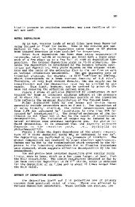
ABSTRACT In this paper, a method of direct electron beam lithographic deposition of metal and metal oxide films is demonstrated using metal organic complexes. In this method, a solution of a metal complex is used to spin coat a substrate to obtain a precursor film. The precursor film is then directly patterned by electron beam writing. A solvent is then used to develop the latent image. Using examples of titanium, tantalum, zirconium, and gold, we illustrate patterning of metal and metal oxide films and both positive and negative deposition. The feature size demonstrated is as low as 14 nm while the demonstrated aspect ratio is as high as 11. INTRODUCTION In this contribution, our recent advances in the direct deposition of metal-containing patterns from metal complexes by electron beam lithography are reported. The prototype of the method is photochemical metal organic deposition (PMOD) [1-3]. In this method, an electron beam, instead of electromagnetic radiation normally used in PMOD, is used to decompose the metal organic precursor. The method is illustrated in Figure 1, where a metal organic precursor film is deposited on a surface, normally by spin coating, an electron beam is then used to produce a latent image on the surface which is then developed. We refer to this method as electron beam induced metal organic deposition (EMOD). Since the energy of accelerated electrons in EMOD is many times higher than that of UV photons, the selected metal organic complex does not have to be photosensitive in the visible or UV region. As a result, a wider selection of precursors is available for EMOD than PMOD. EMOD might also open an opportunity for us to more easily deposit metallic films, as a result of the reducing conditions. a
b
e
c
Figure 1. Direct deposition of metal-containing patterns from metal complexes by electron beam lithography, where a) a metal organic precursor film is coated on the substrate, b) exposed to an electron beam to create a latent image, followed by c) developing to yield the patterned material. Much research has been conducted on alternative methods [1,4-6] to the photoresistassisted lithography for the fabrication of features in nanometer scale. The goal is to directly deposit patterned working layer such as metal wiring or oxide barrier, and therefore, to reduce
cost, material wastes, and pattern transfer errors that associated with dry/wet etch step and photoresist strip step in conventional photolithography. PMOD, compatible with the lithography facilities currently being used in industry, is one of the promising photoresist-free lithography methods. Previously, we have succeeded in the direct lithographic deposition of a number of metals, metal oxides and composites from photosensitive metal organic complexes by PMOD [13,7,8]. We have a
Data Loading...