Synchrotron white beam x-ray topography (SWBXT) and high resolution triple axis diffraction studies on AlN layers grown
- PDF / 500,947 Bytes
- 6 Pages / 612 x 792 pts (letter) Page_size
- 58 Downloads / 293 Views
E8.24.1
Synchrotron white beam x-ray topography (SWBXT) and high resolution triple axis diffraction studies on AlN layers grown on 4H- and 6H-SiC seeds Balaji Raghothamachar1, Michael Dudley1, Rafael Dalmau2, Raoul Schlesser2, Zlatko Sitar2 1
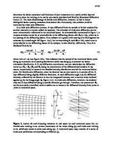
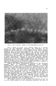
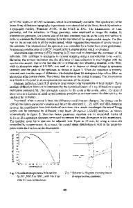
Department of Materials Science & Engineering, SUNY at Stony Brook, Stony Brook, NY 11794-2275, U.S.A. 2 Department of Materials Science & Engineering, North Carolina State University, Raleigh, NC 27695-3419, U.S.A. ABSTRACT For nitride based devices such as LEDs, high power FETs and laser diodes, single crystal substrates of AlN are highly desirable. While the sublimation technique is suitable for growing bulk AlN crystals, appropriate seeds are also necessary for growing large diameter oriented boules. 4H- and 6H-SiC substrates which are readily available commercially can potentially be implemented as seeds for bulk AlN growth. However, issues regarding SiC decomposition at high temperatures, thermal expansion mismatch, single crystal growth, etc. need to be addressed. Towards this end, a series of growth experiments have been carried out in a resistively heated reactor using on and off-axis 4H- and 6H-SiC substrates as seeds for AlN growth from the vapor phase. Several hundred microns thick AlN layers have been grown under different growth conditions. Synchrotron white beam x-ray topography (SWBXT) has been used to map the defect distribution in the grown layers and high resolution triple axis x-ray diffraction (HRTXD) experiments were carried out to record reciprocal space maps from which tilt, mismatch and strain data can be obtained. These results are analyzed with respect to the growth conditions in order to gain a better understanding of this growth process. INTRODUCTION Wide band gap nitride semiconductors are promising materials for a broad range of electronic and opto-electronic devices. Potential applications include electronic devices capable of operation at elevated temperatures, high power or high frequency, and short wavelength optoelectronic devices such as solar blind ultraviolet light detectors, blue light emitting diodes or ultraviolet laser diodes. Currently, some of these applications such as blue LEDs are being realized by growing heteroepitaxial device structures on SiC or sapphire substrates. However, the severe lattice mismatch as well as chemical incompatibility and disparate thermal expansion coefficients degrade the quality of overgrown active nitride layers considerably and limit device lifetime and performance. The high thermal conductivity, large optical bandgap, similar thermal expansion coefficient, and small lattice mismatch of AlN single crystals make it an excellent substrate choice for GaN-based nitride epitaxy. Therefore, there is a great demand for low cost, low dislocation density, large area AlN substrates. While melt growth techniques are precluded for AlN crystal growth because of its extremely high melting point (~3500°K) and the considerable nitrogen pressure required at those temperatures [1], alternative growth techniques such a
Data Loading...