Cross-Sectional Scanning Tunneling Microscopy of Semiconductor Heterostructures
- PDF / 1,616,441 Bytes
- 5 Pages / 576 x 777.6 pts Page_size
- 2 Downloads / 384 Views
we describe the basic experimental techniques involved in cross-sectional STM and give a few representative applications from our work that illustrate the
ability, using cross-sectional STM in conjunction with other experimental techniques, to probe atomic-scale features in the structure of semiconductor heterojunctions and to correlate these features with epitaxial-growth conditions and device behavior.
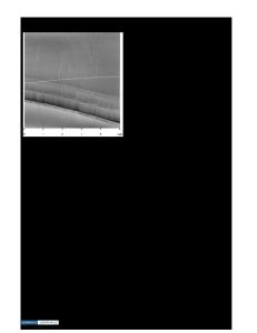
Experimental Considerations In cross-sectional STM, semiconductor wafers are cleaved to expose a cross section—typically a (110) or (111) plane—of epitaxial layers grown or device structures fabricated on the wafer. Scanningtunneling-microscopy experiments performed on the cross-sectional surface can then reveal information about the atomic-scale morphology and electronic structure of these epitaxial layers or devices. Figure 1 shows the typical geometry of the sample and STM probe tip in cross-sectional STM; a schematic illustration of the atomic structure of the sample and probe tip near the (110) cleaved surface of a zincblende semiconductor; and a representative, atomically resolved cross-sectional STM image of an InAs/Gai ,In,Sb superlattice structure obtained in our laboratory.
(001)
t
epi layers
• anion O cation O metal atom (tip)
[iTo;
STM tip sample
Figure 1. Sample and probe-tip geometry, arrangement of atoms in the sample and tip, and a representative image in cross-sectional scanning tunneling microscopy (STM). Typically an (001) semiconductor wafer is cleaved to expose a (110) cross-sectional surface. Tunneling measurements are then performed with the STM tip positioned over the region of interest—generally consisting of exposed cross sections of epitaxial layers grown or devices fabricated on the top of the wafer—on the cross-sectional surface. The image shown corresponds to filled states in a (110) cross section of an lnAs/Ga075ln0,25Sb superlattice.
MRS BULLETIN/AUGUST 1997
Cross-Sectional Scanning Tunneling Microscopy of Semiconductor Heterostructures
As indicated schematically in Figure 1, the cation and anion sites in the {110} surface planes of compound semiconductors contain unoccupied and occupied dangling-bond states, respectively. Scanning-tunneling-microscopy imaging of the GaAs(llO) surface has shown that for positive bias voltage applied to the sample, one obtains images of the unoccupied orbitals corresponding to the Ga (cation) sites on the (110) surface; for negative sample bias voltage, one images the occupied orbitals corresponding to the As (anion) sublattice on the (110) surface.10 Detailed STM studies of the GaAs(llO) surface have shown that the surface unit cell remains 1 X 1, with the surface reconstruction consisting only of some buckling and bond reorientation.10 For Group-IV elemental semiconductors, achieving atomically flat cleaved surfaces is problematic and the as-cleaved (110) surface has been found to be disordered11 with complex surface reconstructions appearing upon annealing at high temperature.1213 However hydrogen passivation of the (110) surface can b
Data Loading...