How the sputtering process influence structural, optical, and electrical properties of Zn 3 N 2 films?
- PDF / 659,674 Bytes
- 8 Pages / 612 x 792 pts (letter) Page_size
- 92 Downloads / 413 Views
Prospective Article
How the sputtering process influence structural, optical, and electrical properties of Zn3N2 films? Junjun Jia, and Hironori Kamijo, Graduate School of Science and Engineering, Aoyama Gakuin University, 5-10-1, Fuchinobe, Chuo, Sagamihara, Kanagawa 252-5258, Japan Shin-ichi Nakamura, Center for Instrumental Analysis, College of Science and Engineering, Aoyama Gakuin University, 5-10-1, Fuchinobe, Chuo, Sagamihara, Kanagawa 252-5258, Japan Yuzo Shigesato, Graduate School of Science and Engineering, Aoyama Gakuin University, 5-10-1, Fuchinobe, Chuo, Sagamihara, Kanagawa 252-5258, Japan Address all correspondence to [email protected] (Received 24 January 2018; accepted 22 March 2018)
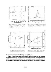
Abstract The use of zinc nitride (Zn3N2) films as a transparent electrode in various electronic devices has attracted much attention owing to its highcarrier mobility. In this study, we investigate the influence of the sputtering process on structural, optical, and electrical properties of a Zn3N2 film deposited by reactive magnetron sputtering. The reactivity of nitrogen species can be improved by changing the type of sputtering gas. Compared with Ar or Ne sputtering gas, polycrystalline Zn3N2 films deposited using He sputtering gas have a larger grain size. The optical band gap of the Zn3N2 films varied from ∼1.2 to 1.5 eV depending on the N2 flow ratio and type of sputtering gas. The maximum mobility was 91.1 cm2/Vs when the Zn3N2 film was deposited using Ar sputtering gas with an N2 flow ratio of 40%. The carrier density of Zn3N2 films deposited using Ar sputtering gas was notably higher than those deposited using Ne or He sputtering gas, and more oxygen atoms are considered to substitute into nitrogen sites, where oxygen is considered to be from the residual water vapor in the sputtering chamber.
Introduction Group III nitride semiconductors, including GaN, InN, and AlN, have been recognized in both theory and practice as one of the most useful materials in electronic devices, such as light-emitting diodes (LEDs) and power-electronic devices.[1–3] However, fewer studies about group II nitride semiconductors have been published than about group III nitrides.[1–3] Our present study focuses on group II semiconductors, i.e., zinc nitride (Zn3N2) thin films, composed of inexpensive and earth-abundant Zn and N elements. Zn3N2 has a cubic anti-bixbyite crystal structure[4] and is highly transparent in the visible to near-infrared regions because it has a wide band gap and large refractive index. Therefore, Zn3N2 can be utilized as a transparent electrode in solar cells or GaN-LEDs. Futsuhara et al. reported that synthetic polycrystalline Zn3N2 films exhibit a high electron mobility of ∼100 cm2/Vs with the n-type character at room temperature.[5]The highest reported mobility is 395 cm2/Vs.[6] Cao et al. explained that such a high mobility is attributed to the small effective electron mass of Zn3N2.[7,8] However, several studies showed that the optical band gap of Zn3N2 films varies from 1.1 to 3.2 eV.[9–12] Such a large inconsis
Data Loading...