Imaging of stacking faults in highly oriented pyrolytic graphite using scanning tunneling microscopy
- PDF / 747,670 Bytes
- 4 Pages / 576 x 792 pts Page_size
- 63 Downloads / 334 Views
Scanning tunneling microscopy images of the (0001) plane of highly oriented pyrolytic graphite show defect regions consisting of an extensive network of partial dislocations that form extended and contracted nodes. The partial dislocations in hexagonal graphite enclose triangular regions (~1000 nm on a side) of faulted material comprised of rhombohedral graphite. Electronic and elastic interactions of the tip with the HOPG surface are proposed to explain the observed image contrast between hexagonal and rhombohedral graphite.
I. INTRODUCTION Highly oriented pyrolytic graphite (HOPG) is used extensively as a substrate and calibration standard in scanning tunneling microscopy (STM). In spite of its widespread use, characterization of the structural and electronic properties of graphite using STM and tunneling spectroscopy (TS) has been difficult, due in part to the crystalline disorder in commercial polycrystalline HOPG samples used for STM studies.1"14 Reports have documented unusual observations of graphite in scanning tunneling microscopy images, such as "giant corrugations",1>2(a)'9>14 large tunneling current asymmetries between adjacent carbon atoms,2(h)'12'13 and large-scale hexagonal patterns rotated at various angles with respect to the normal atomic corrugations.3'4 Explanations for these anomalies are still being forwarded, although no conclusive answers have been agreed upon. Here, we report an extensive triangular network found in STM images of the (0001) plane of HOPG and discuss several possible explanations for the contrast mechanism observed in these images. Comparison of the present STM images with previous transmission electron microscopy (TEM) images of HOPG suggests that the observed extended network is an array of alternating hexagonal and rhombohedral graphite. II. PROCEDURES AND RESULTS Tunneling experiments were performed on a freshly cleaved sample of HOPG (grade B from Union Carbide). A commercial STM (Nanoscope II, Digital Instruments Inc.) was used to acquire constant current images and current-voltage (I-V) curves in air. STM tips were made by mechanically cutting Pt-Rh (80-20%) wire. Images reported here were recorded using a bias voltage of 30 mV (sample versus tip), a set-point current of 1.1 nA, and a scan rate of 4.34 Hz. J. Mater. Res., Vol. 7, No. 2, Feb 1992
http://journals.cambridge.org
Downloaded: 14 Mar 2015
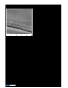
Figures l(a) and l(b) are STM images of an array of triangles on the (0001) surface of HOPG. STM images of arrays similar to these are occasionally observed in our laboratory when using HOPG as a substrate for STM studies. The defect region, which is in excess of 4000 nm x 4000 nm, begins at a cleavage step [lower left corner of Fig. l(b)]. The triangles increase in size with distance away from the step. The triangular shapes range from equilateral triangles to triangles where one of the corners extends into a long ribbon. Within the array, the light triangles appear displaced above the darker triangular regions by ~ 4 A. Three triangles intersect forming a bright point
Data Loading...


