Impact of CMOS TiN metal gate process on microstructure and its correlation with electrical properties
- PDF / 1,121,591 Bytes
- 7 Pages / 432 x 648 pts Page_size
- 8 Downloads / 397 Views
MRS Advances © 2019 Materials Research Society DOI: 10.1557/adv.2019.77
Impact of CMOS TiN metal gate process on microstructure and its correlation with electrical properties Pushpendra Kumar1,2,3, Florian Domengie1, Charles Leroux2, Patrice Gergaud2, G. Ghibaudo3 1
STMicroelectronics, 850 rue Jean Monnet, 38926, Crolles Cedex, France
2
Univ. Grenoble Alpes, CEA, LETI, 38000 Grenoble, France,
3
IMEP-LAHC, Minatec/INPG, BP 257, 38016 Grenoble, France
ABSTRACT
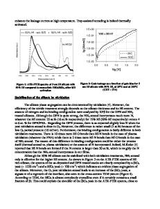
In this paper, the effect of TiN metal gate deposition conditions on the crystal orientation and size of TiN grains has been investigated. We have focused on process conditions that reduce the grain size or provide a unique orientation, which might impact CMOS threshold voltage variability. We have shown that the grain size can be significantly modulated by the RF power and pressure, with grain size as low as 5.2 nm. Further it has been shown that for a few optimized conditions, a unique grain orientation can be obtained. Then, the impact of these process conditions on TiN gate mechanical stress and electrical properties has been investigated. Mechanical stress and sheet resistance are modulated by pressure and RF power and have been correlated to the deposition rate and TiN grain size respectively. The effect of TiN process conditions on MOS capacitor effective workfunction (WFeff) has been investigated, and the trend is opposite to the expected modulation of the intrinsic TiN metal gate workfunction with grain orientation. On the contrary, WFeff variation is well correlated to the Ti/N ratio, suggesting an effect related to dipole at the SiO2/high-k interface.
INTRODUCTION High-k metal gate (HKMG) stack has been used in order to continue the aggressive scaling of MOS transistors. The introduction of the TiN metal gate has advantages such as eliminating Fermi level pinning and phonon scattering, but it also
Downloaded from https://www.cambridge.org/core. Iowa State University Library, on 03 Feb 2019 at 12:48:06, subject to the Cambridge Core terms of use, available at https://www.cambridge.org/core/terms. https://doi.org/10.1557/adv.2019.77
introduces the metal gate granularity. TiN metal film grain microstructure may impact the physical and electrical properties of the device, such as mechanical stress, sheet resistance, effective workfunction (WFeff) and threshold voltage local variability (σVTH). These properties will have an impact on device performance. TiN metal grains with different crystallographic orientations have different intrinsic work functions (WFM) at the interface between metal and high-k, the two well-known ones are and having WFM values of 4.4 eV and 4.6 eV respectively. Relative proportion of these grains might impact WFeff and σVTH. In previous studies, σVTH has been shown to be related to the metal gate microstructure [1]. σVTH might be reduced by obtaining an amorphous microstructure [2], reducing the grain size or by obtaining a unique crystal orientation. In this paper, we focus on identifying TiN metal gate process conditi
Data Loading...