In-line Monitoring of Grain Size Distribution of Channel Poly Si used in 3D NAND Flash Memory Devices using Multiwavelen
- PDF / 1,185,750 Bytes
- 11 Pages / 432 x 648 pts Page_size
- 12 Downloads / 289 Views
Advances:
Email alerts: Click here Subscriptions: Click here Commercial reprints: Click here Terms of use : Click here
In-line Monitoring of Grain Size Distribution of Channel Poly Si used in 3D NAND Flash Memory Devices using Multiwavelength Raman Spectroscopy Noh Yeal Kwak, Chul Young Ham, Min Sung Ko, Sung Chul Shin, Seung Jin Yeom, Chul Woo Park, Chun Ho Kang, Byung Seok Lee, Sung Gi Park, Noh Jung Kwak and Woo Sik Yoo MRS Advances / Volume 1 / Issue 05 / January 2016, pp 339 - 348 DOI: 10.1557/adv.2016.1, Published online: 18 January 2016
Link to this article: http://journals.cambridge.org/abstract_S2059852116000013 How to cite this article: Noh Yeal Kwak, Chul Young Ham, Min Sung Ko, Sung Chul Shin, Seung Jin Yeom, Chul Woo Park, Chun Ho Kang, Byung Seok Lee, Sung Gi Park, Noh Jung Kwak and Woo Sik Yoo (2016). In-line Monitoring of Grain Size Distribution of Channel Poly Si used in 3D NAND Flash Memory Devices using Multiwavelength Raman Spectroscopy. MRS Advances, 1, pp 339-348 doi:10.1557/adv.2016.1 Request Permissions : Click here
Downloaded from http://journals.cambridge.org/ADV, IP address: 128.210.126.199 on 24 May 2016
MRS Advances © 2016 Materials Research Society DOI: 10.1557/adv.2016.1
In-line Monitoring of Grain Size Distribution of Channel Poly Si used in 3D NAND Flash Memory Devices using Multiwavelength Raman Spectroscopy Noh Yeal Kwak1, Chul Young Ham1, Min Sung Ko1, Sung Chul Shin1, Seung Jin Yeom1, Chul Woo Park1, Chun Ho Kang1, Byung Seok Lee1, Sung Gi Park1, Noh Jung Kwak1, Woo Sik Yoo2 1
FEPT Technology Group, manufacturing & Technology Division, SK hynix, Icheon-si, Gyeonggi-do, 467-701, Korea
2
WaferMasters, Inc., 254 East Gish Road, San Jose, CA 95112, USA
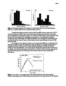
ABSTRACT Feasibility of multiwavelength Raman spectroscopy was studied as a potential in-line monitoring technique for grain size distribution in channel poly-Si used in three dimensional stacked NAND (3D NAND) Flash memory devices. Various channel poly-Si materials in 3DNAND Flash memory devices, converted from chemical vapor deposition (CVD) grown a-Si, were characterized using non-contact, multiwavelength Raman spectroscopy and high resolution cross-sectional transmission electron microscopy (HRXTEM). The Raman characterization results were compared with HRXTEM images. The correlation between the grain size distribution characterized by multiwavelength Raman spectroscopy and “on current” (ION) of 3D NAND Flash memory devices was investigated. Good correlation between these techniques was seen. Multiwavelength Raman spectroscopy is very promising as a non-destructive in-line monitoring technique for grain size distribution in channel poly-Si used in 3D NAND Flash memory devices. INTRODUCTION For three dimensional vertically stacked NAND (3D NAND) Flash memory devices, device scaling is being achieved by vertical staking of thin film transistors (TFTs) in multiple layer configurations, without heavily relying on advances in lithography. 3D NAND Flash memory device fabrication involves many processes that have never before
Data Loading...