Indium Gallium Arsenide Based Non-Volatile Memory Devices with Site-Specific Self-Assembled Germanium Quantum Dot Gate
- PDF / 546,941 Bytes
- 6 Pages / 612 x 792 pts (letter) Page_size
- 74 Downloads / 368 Views
1250-G01-05
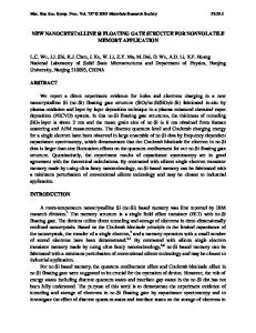
Indium Gallium Arsenide Based Non-Volatile Memory Devices with Site-Specific SelfAssembled Germanium Quantum Dot Gate Pik-Yiu Chan, Mukesh. Gogna, Ernesto Suarez, Fuad Al-Amoody, Supriya Karmakar ,Barry I. Miller, John E. Ayers, and Faquir C. Jain Department of Electrical and Computer Engineering, University of Connecticut, 371 Fairfield Way, U-2157, Storrs, CT 06269, U.S.A. ABSTRACT This paper presents the implementation of indium gallium arsenide field-effect transistors (InGaAs FETs) as non-volatile memory using lattice-matched II-VI gate insulator and quantum dots of GeOx-cladded Ge as the floating gate. Studies have been done to show the ability of IIVI materials to act as a tunneling gate material for InGaAs based FETs, and GeOx-cladded Ge quantum dots having the ability to store charges in the floating gate of a memory device. Proposed structure of the InGaAs device is presented. INTRODUCTION Recently, there have been many reports of implementing InGaAs FETs either on InP or directly on Si substrates. Due to its high electron mobility, indium gallium arsenide high electron mobility transistors (HEMTs) are one of the fastest transistors on the market. Unlike HEMTs, InGaAs FETs in MOS or CMOS configuration require the use of a gate insulator that provides minimum interface states resulting in reproducible threshold voltage behavior. Finding an appropriate gate oxide for InGaAs based CMOS devices is challenging. Jain, et. al. have shown that using high-k II-VI materials that are lattice-matched to the InGaAs material serves as a good gate insulator for such devices [1]. Scaling of CMOS devices is also another problem currently faced by the memory industry. Thinner gate material means faster operating speed of the memory device, but it can also increase current leakage in the device. Memory devices with silicon nanocrystals as the floating gate have long been introduced [2]. These silicon nanocrystals act as the charge storage units, but retention of these charges become a problem. To solve this problem, cladded nanocrystals have been used as the floating gate of the memory devices [3, 4]. This study combines the use of high-k II-VI materials as the gate insulator and the cladded nanocrystals as the floating gate to create a new type of InGaAs non-volatile memory. EXPERIMENTAL DETAILS Figure 1 shows the cross-sectional schematic of the InGaAs non-volatile memory device. The starting substrate was a 2000Ǻ InGaAs layer grown on an InP substrate by metalorganic chemical vapor deposition (MOCVD). The InGaAs layer was doped p-type by introducing zinc during the growth. The deposition was done at 635oC, and the p-type doping was about 1016/cm3. 5000Ǻ of PECVD oxide was deposited on the InGaAs layer to act as a masking oxide. The pattern of the source and drain regions was formed, and the p-InGaAs regions were
G S
D
PECVD oxide GeOx-cladded Ge quantum dots II-VI gate insulator PECVD oxide
n+
n+
p-InGaAs Figure 1. Cross-sectional schematic of the InGaAs non-volatile memory with GeOx-cladded Ge quantum
Data Loading...