Layout Pattern Density and Oxide Deposition Profile Effects on Dielectrics CMP
- PDF / 179,543 Bytes
- 6 Pages / 612 x 792 pts (letter) Page_size
- 38 Downloads / 276 Views
Layout Pattern Density and Oxide Deposition Profile Effects on Dielectrics CMP Young B. Park, Joon Y. Kim, and Dae W. Seo System IC R & D Center, Hyundai Electronics Co., Ltd., Cheongju, 360-480, Korea ABSTRACT Test mask for characterizing pattern dependent variation of the remaining thickness after chemical-mechanical polishing (CMP) was designed with taking the experimentally obtained interaction distance into consideration. Measured interaction distance was constant independent of pattern variables such as pattern density and pattern shapes between line and area. And systematic exploration regarding pitch effects on remaining nitride thickness in STI (Shallow Trench Isolation) CMP was performed with comparing PETEOS (Plasma Enhanced Tetra Ethyl Ortho Silicate) and HDP (High Density Plasma) oxide. Both measured remaining nitride thickness and expected oxide pattern density from consideration of deposition profile effects showed a good correlation with respect to pitch variation for a constant layout pattern density.
INTRODUCTION CMP has been an important process in dielectric planarization, shallow trench isolation, and metal damascene processes. CMP is very sensitive to the pattern density, but the concept of pattern density is not numerically well defined for oxide film, especially for HDP film or multilayer dielectric film [1-4]. So, a clear definition of pattern density is necessary to proceed the CMP modeling. It was recently reported that topographic profile differences between HDP and conformal CVD oxide would result in different pattern density for each oxide from that of design layout [5]. But there has been few experimental data for these deposition profile effects on CMP, especially for pith variations at a constant layout density. In this paper, interaction distance was measured with pattern variables such as pattern density and pattern shapes between line and area. And using test mask with taking measured interaction distance into consideration, polishing behavior between PETEOS and HDP oxide are compared to investigate the deposition profile effects in STI CMP. EXPERIMENTAL DETAILS Generally, the low-density region will polish faster than the high-density region with a M5.4.1
transition ramp in between the two regions with a step change in pattern density. Interaction distance for CMP process is defined to be the width of this transition ramp [4]. Therefore, interaction distance can be physically interpreted as the macroscopic distance over which the pad bends and conforms to the wafer surface [4]. At first, interaction distance was directly measured from step density test mask, which contains large step change in pattern density. This step density mask has several square blocks of 12mm length with the space of 10mm where pattern density, pitch, and pattern shape between line and square are varied along each pattern block. A short loop process sequence prior to CMP was performed on 200mm wafers using following flow; blanket deposition of PETEOS and patterning using step density mask, followed by d
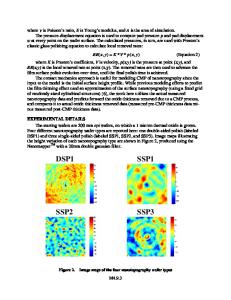
Data Loading...