Line-Width Dependence of Void Formation in Ti-Salicided BF 2 -Doped Polysilicon Lines
- PDF / 1,637,960 Bytes
- 9 Pages / 417.6 x 639 pts Page_size
- 42 Downloads / 275 Views
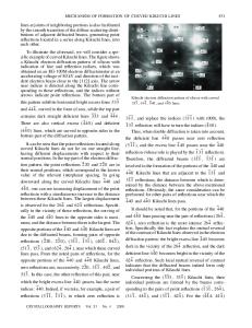
CoSi 2 and NiSi 2 on BF 2+-implanted silicon [2-4]. Lur et al. [2] also reported that the density of both dislocations and fluorine bubbles decreased with increasing annealing temperature. However, the size of both dislocations and fluorine bubbles showed the reverse trend. In addition, Lur et al. found that with further increase in temperature, large fluorine bubbles were concentrated near the TiSi 2/Si interface. However, no evidence of fluorine bubbles could be found within the silicide layers. In all these studies, the focus was on the blanket samples in which the impact of localized stress associated with the neighboring structures was not considered. We report the first observation of voids in sub-quarter-micron Ti-salicided BF 2-doped polySi local interconnect lines. The formation of these voids was found to be dependent on the BF 2 implant dose, the activation annealing as well as the polySi line-width. So far, the results indicate that fluorine, or possibily SiFx precipitates, is the main cause to the voiding observed. It was also found that this voiding phenomenon was aggravated by the localized mechanical stress from the side-wall nitride spacers. However, the actual void evolution process in these sub-quarter-micron polySi structures has not yet been well-understood. In addition, not much attention has been paid to the effect on fluorine segregation in the presence of highly localized lateral stress in TiSi 2/polySi-gate system due to the side-wall spacers. On the other hand, the evolution of fluorine bubbles due to accumulation of fluorine 91 Mat. Res. Soc. Symp. Proc. Vol. 564 © 1999 Materials Research Society
atoms at the polySi/Si system after a BF 2+-implant at a dose ranging from 1.00xlO05 to 6.00xlO15 cm- has been well documented [5-11 ]. In this paper, effect of the polySi gate line-width on the physical properties of the observed voids in TiSi 2 films is reported. The void density and its distribution, and the impact of the inwards stress from the side-wall nitride spacers on the void in the TiSi 2/polySi layered structures were examined by SEM and XTEM. An attempt is made to explain the void phenomenon seen in TiSi 2 through a simple schematic showing a possible physical mechanism. EXPERIMENTS p-type Si(100) wafers with resistivity of 0.5 - 100 0)-cm were used as the starting substrates for the formation of Ti-salicided p÷ polySi lines. PolySi lines with line-widths ranging from 0.18 ýim to 0.50 ý.im were patterned, after which TEOS liners and silicon nitride (Si 3N 4) layers were deposited and subsequently etched to form the side-wall nitride spacers. The polySi lines were implanted with a BF 2 dose of 3.00x10 15 cm-2 and rapid thermal annealed (RTA) at 1030 TC for 30 seconds. For pre-amorphization implantation (PAl) and implantthrough-metal (ITM) enhancement techniques, 28Si÷ was used as the implantation species. In all cases, the as-deposited Ti thickness was kept at 400 A. Upon deposition, the wafers were rapid thermal annealed at 775 TC in a N 2 ambient for 30 seconds to form the TiSi 2
Data Loading...