Linear Zone-Melt Recrystallized Si Films using Incoherent Light
- PDF / 1,803,632 Bytes
- 6 Pages / 417.6 x 639 pts Page_size
- 61 Downloads / 312 Views
LINEAR ZONE-MELT RECRYSTALLIZED Si FILMS USING INCOHERENT LIGHT
AVID KAMGAR, G. A. ROZGONYI* AND R. KNOELL Bell Laboratories, Murray Hill, New Jersey
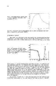
ABSTRACT Incoherent tungsten radiation has been used to recrystallize polysilicon films deposited on SiO 2, grown on 75 mm diameter wafers. These films have been analyzed by a variety of techniques such as optical microscopy, Auger spectroscopy and TEM crosssectioning. These films are large (> 50 mm dia.) single crystals, and contain fewer defects and impurities than similar films recrystallized in graphite strip heater ovens. They do, however, contain the subgrain boundaries found previously, even when high purity MBE polysilicon is used. In vertical TEM cross-sectioning, in addition to the subgrain boundaries, we have seen crystallized particles of 50200 A size in the Si film at both the upper and lower SiO 2 boundaries. Although these particles could be related to formation of the subgrain boundaries, no definite correlation has been made.
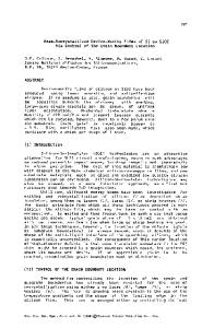
INTRODUCTION Potential advantages of silicon films on insulating substrates (SO) as an alternative to silicon on sapphire (SOS) for fabricating high speed, radiation hard circuits have created much interest in the SOI technology. Many laboratories are investigating the recrystallization of Si films using various techniques such as lasers [1], electron beams [21 graphite strip heaters [3-51 and incoherent light [6-81. Recently we reported successful recrystallization of large area single crystal films on oxidized three inch wafers using tungsten lamps [6]. Here we will present additional structural and chemical analysis of these films using optical microscopy, Auger spectroscopy, and horizontal and vertical cross-sectional transmission electron microscopy (TEM) in a Philips model 400 equipped with EDAX (energy dispersion analysis by x-ray). EXPERIMENT Figure 1(a) illustrates the three main parts of the system. The wafer is housed in a rectangular quartz tubing which is flushed by argon. A high intensity panel light, employing six tungsten lamps, heats the wafer from the bottom to 1000-1300*C. A lineheater provides the additional heat, from the top, for melting the polysilicon. The lineheater consists of a tungsten lamp and two elliptical reflectors which focus the light into a narrow strip. In this configuration the line heater is drawn by a motor, at the desired * North Carolina State University, Raleigh, NC. Mat.
Res.
Soc. Symp.
Proc.
Vol.
13 (1983) QElsevier
Science Publishing Co.,
Inc.
570
(a) Ar
(b)
I
I
3 INCH
(C)
o
POLYSILICON
05M
Fig. 1
Si (400)
2
SIF
m
Schematic view of the recrystallization system (a), and the multi-layered wafer (b) and (c).
speed, to drag the molten zone from the single crystal edge of the wafer to the end. A detailed description of the system can be found in Ref. [6]. The multi-layered structure was fabricated on 75 mm diameter (100) Si wafers as shown schematically in Figs. 1(b) and (c). The planar structure was obtained by using Si 3 N 4 as an edge mask while - 1 Am of the
Data Loading...